SLVAF84 September 2021 DRV8311 , DRV8312 , DRV8313 , DRV8316 , DRV8332 , MCT8316Z
3 Additional Dead Time From the MCU PWM Inputs
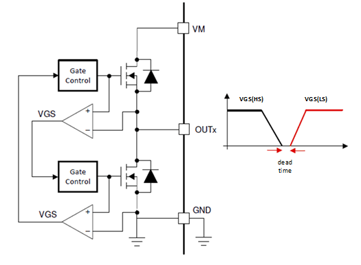
Many gate drivers and integrated FET drivers in the DRV8x family integrate automatic dead time insertion to prevention cross-conduction and shoot-through of the half-bridge driver (Figure 3-1). This is accomplished via handshaking between the gate-to-source voltage of the high-side and low-side gate drivers, which is internal in integrated MOSFET drivers. Dead time is dependent on the slew rate setting of the device, and it is specified with typical and maximum values.
 Figure 3-1 Definition of Dead Time in Integrated MOSFET Drivers
Some designers prefer to additionally include dead time from the PWM outputs of the microcontroller as an extra precaution for shoot-through protection. This creates a condition where internal logic prioritizes the MCU dead time or driver dead time based on their durations.
Typically, if the MCU dead time is less than the driver dead time, the driver will compensate and make the true output dead time the value specified by the DRV device. Conversely, if the MCU dead time is larger than the driver dead time, then the driver will adjust accordingly to the MCU dead time as shown in Table 4-1.