SLUUC27C June 2019 – July 2022 BQ25611D , BQ25619
4.1 Board Layout
Figure 4-1 through Figure 4-8 illustrate the PCB board layouts.
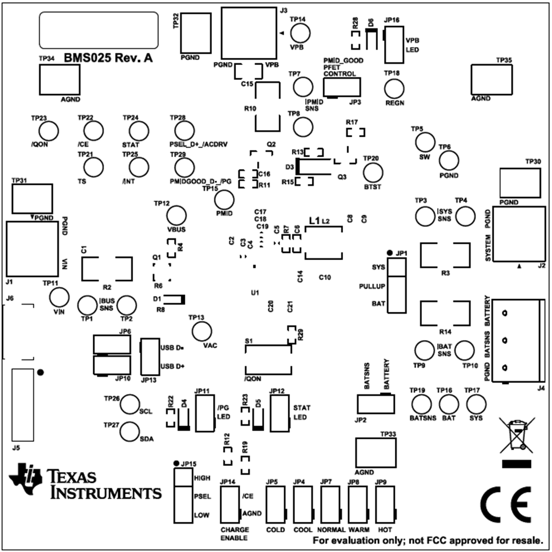 Figure 4-1 BMS025 Rev. A Top Overlay
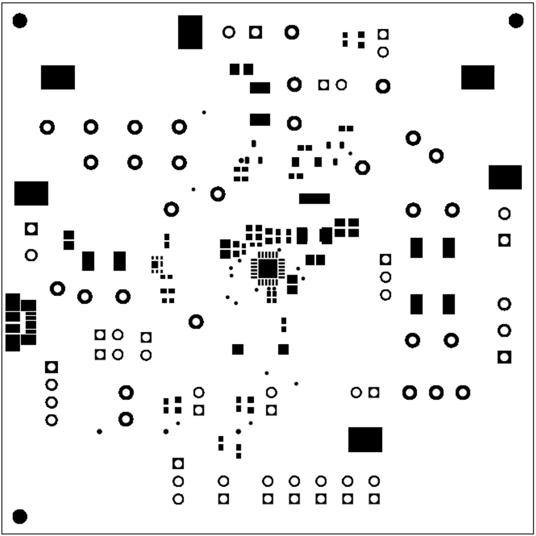 Figure 4-2 BMS025 Rev. A Top Solder Mask
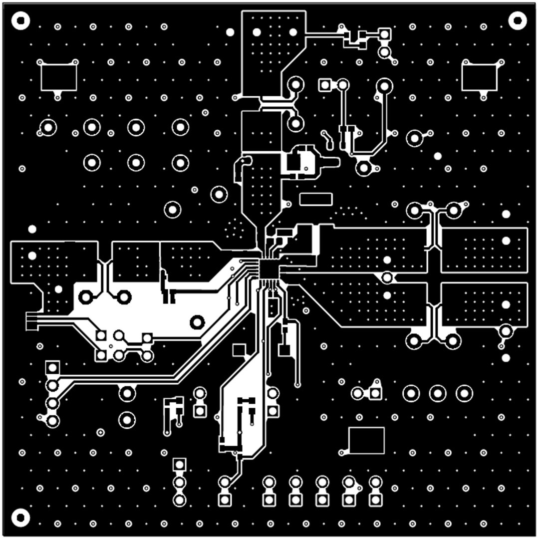 Figure 4-3 BMS025 Rev. A Top Layer
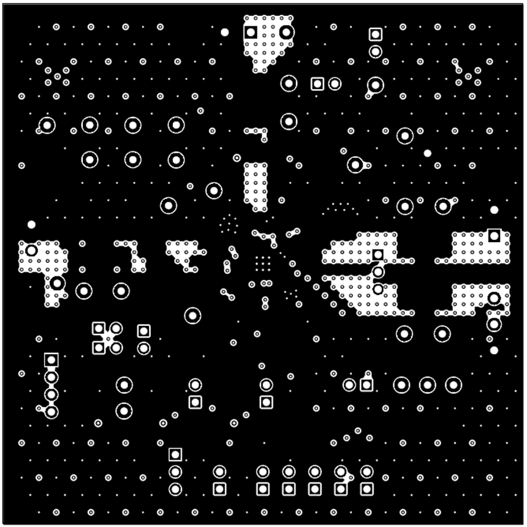 Figure 4-4 BMS025 Rev. A MidLayer 1
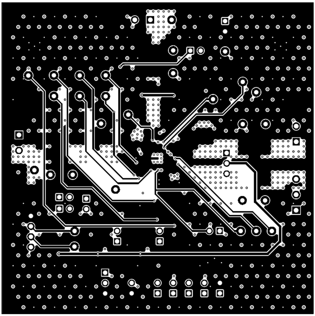 Figure 4-5 BMS025 Rev. A MidLayer 2
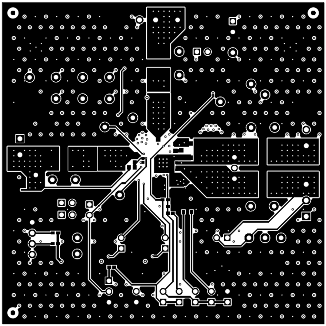 Figure 4-6 BMS025 Rev. A Bottom Layer
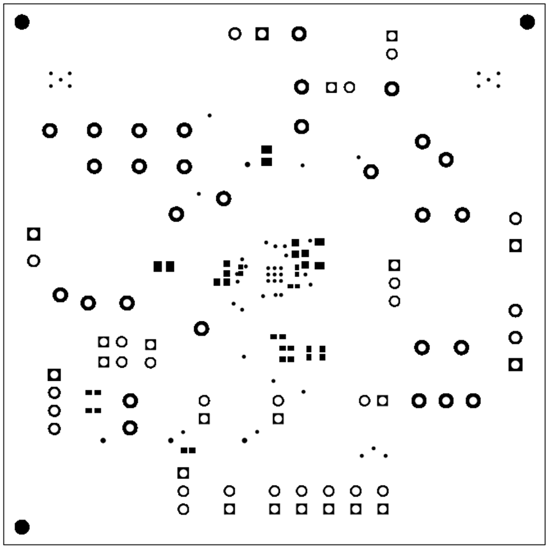 Figure 4-7 BMS025 Rev. A Bottom Solder Mask
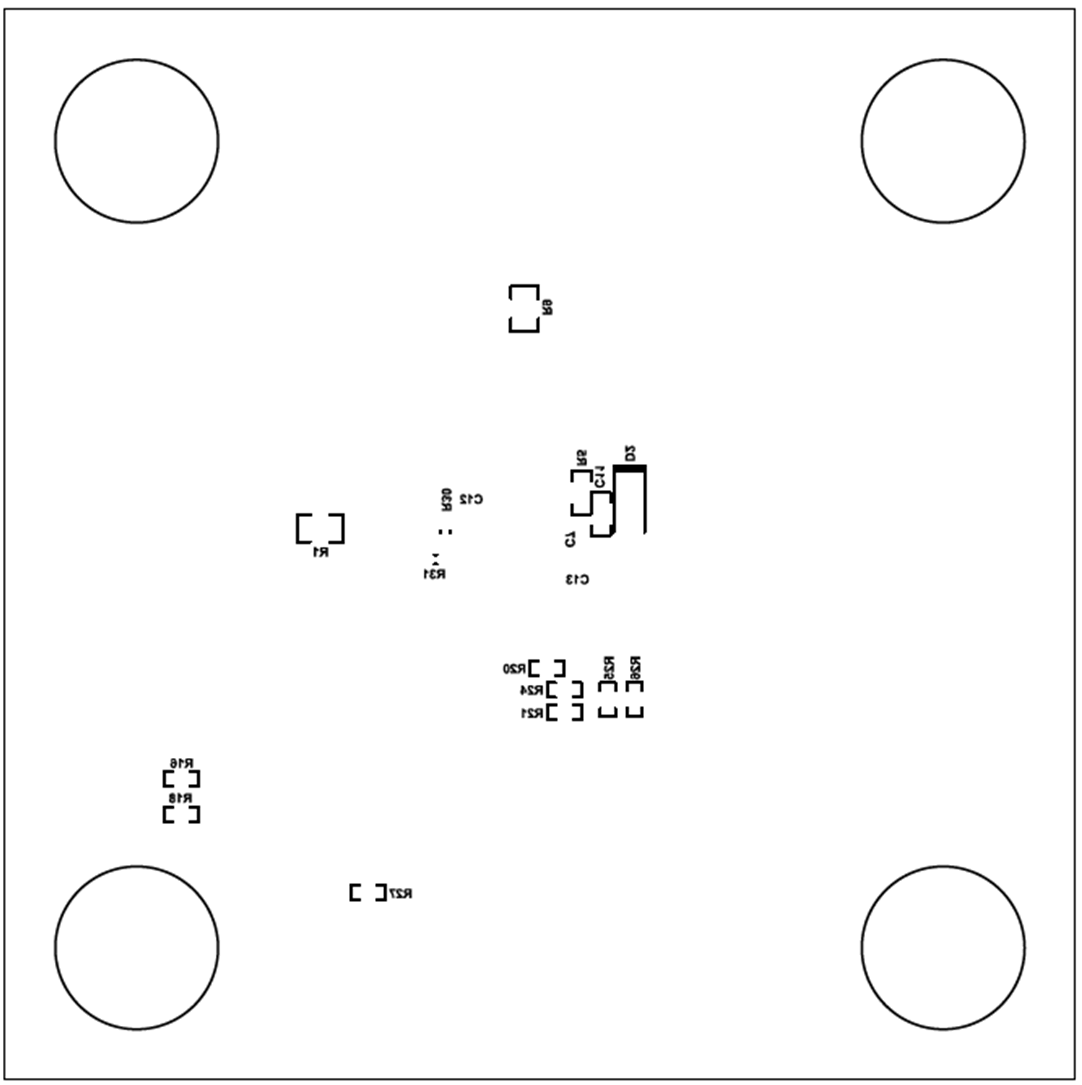 Figure 4-8 BMS025 Rev. A Bottom Overlay