SLUAAC5 August 2021 UCC28700 , UCC28701 , UCC28702 , UCC28703 , UCC28704 , UCC28710 , UCC28711 , UCC28712 , UCC28713 , UCC28720 , UCC28722 , UCC28730 , UCC28740 , UCC28742 , UCC28910 , UCC28911
- Trademarks
- 1 Introduction
- 2 Brief Review of DCM FM, AM, FM Flyback Control Law
- 3 Input (VIN) and Output (VOUT) Voltage Sensing for UVLO and OVP Fault Protection
- 4 Input Under Voltage Lockout (UVLO) Protection
- 5 Output Overvoltage (OVP) Protection
- 6 Not Recognizing a UVLO or OVP Fault
- 7 Separate Bias Supply Startup Issue and Resolution
- 8 Not Having a Clean Aux Winding Signal
- 9 Removing Aux Winding Ringing to Resolve False Triggering of OVP and UVLO Faults
- 10Noise on CS Pin Tripping Over Current Protection (OCP)
- 11Summary
- 12References
9 Removing Aux Winding Ringing to Resolve False Triggering of OVP and UVLO Faults
Parasitic inductances and capacitances are the major cause of aux winding ringing that can falsely trip OVP is in the design. To help reduce this ringing it is recommended through layout and transformer design that you keep the parasitic inductances and capacitances as small as possible.
The layout section (Section 10) of UCC28704 data sheet (SLUSCA8A) gives recommendations on how to layout the PSR flyback with minimal trace inductance and capacitance. It also has a layout that was constructed based on these recommendations in section 10.2, SLUSCA8.
When selecting and or designing your transformer (T1) it is recommended that a transformer have a primary leakage inductance (LPLK) of less than three percent of the primary magnetizing inductance (LPM), Figure 1-1. This will help to reduce ringing at the switch nodes.
During layout process, keep the PCB traces in the power stage; as short as, possible. Keep in mind that every inch of trace adds roughly 10 nH of parasitic trace inductance (LTRACE). Keeping the traces as short as possible removes unwanted antennas from the design helping to improve noise impunity as well..
Use an RCD clamp (RA , RC, CA, DA) over a TVS clamp (DA, DZ), (Figure 1-1). An RCD clamp will provide dampening at the switch node, where TVS clamp will only clamp the voltage when the switch node rings above the clamp voltage and provides very little to no dampening. Set the RA and CA time constant of the clamp to greater than 10 times the maximum switching period, Equation 14 and Equation 15. Please note for safety the designer want to use DZ to clamp VSW as well.
To reduce excessive ringing across the secondary (VSEC ) winding it will couple into VAUX through the auxiliary to primary turns ratio. The waveform presented in Figure 9-1 shows ringing on the secondary of simulated from a 390 V to 12 V, 10 W, flyback converter. Excessive ringing present on VSEC will couple onto VAUX and if it severe enough can cause and OVP. As a result, the design will not lose output voltage regulation causing the design to misbehave.
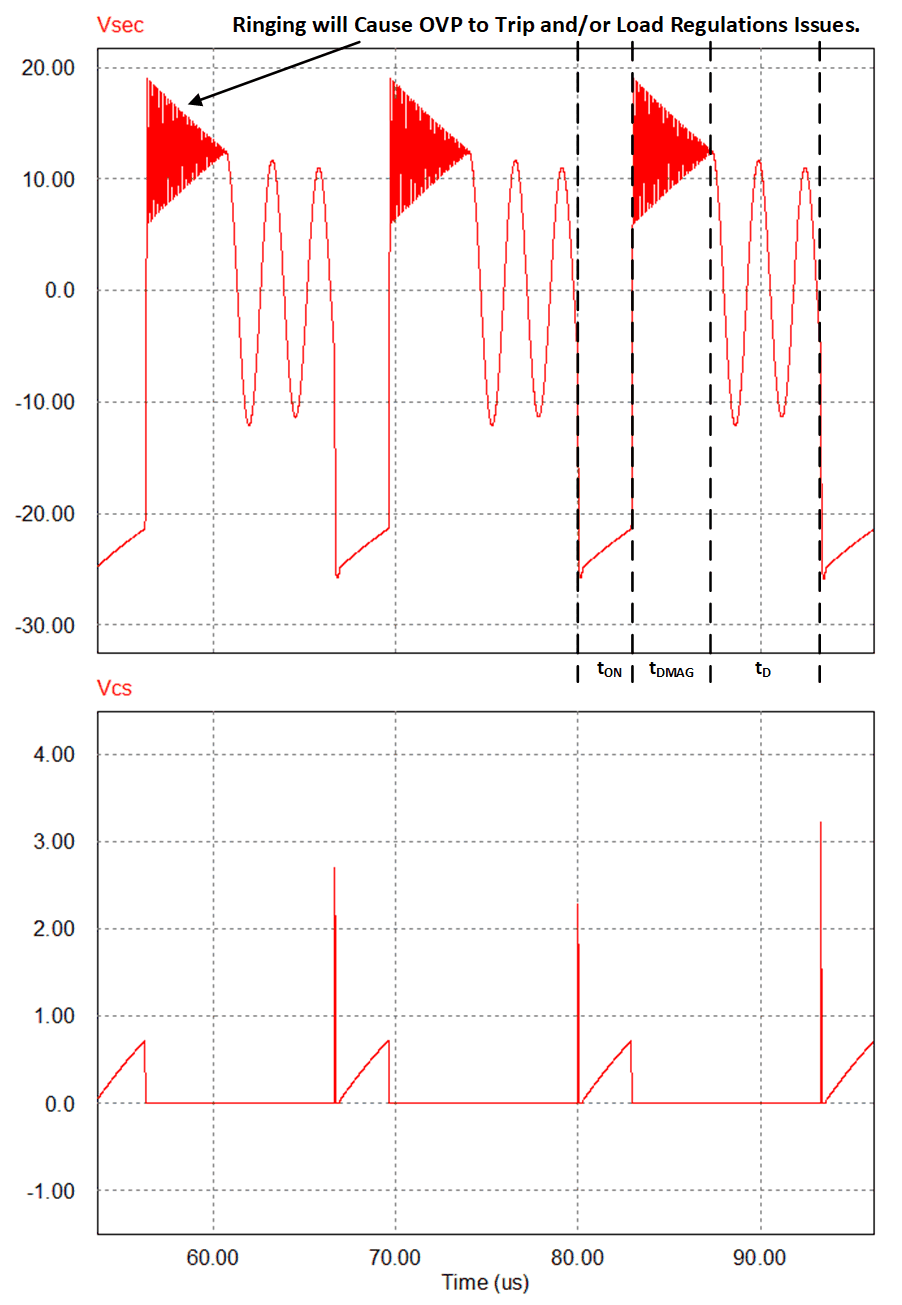 Figure 9-1 Flyback Secondary Voltage with
Excessive Ringing
Figure 9-1 Flyback Secondary Voltage with
Excessive RingingThe cycle by cycle energy transfer between parasitic leakage inductances and parasitic switch node capacitances causes ringing at the flyback converter switch nodes. This ringing will couple through the flyback converter’s switch nodes to VAUX. Excessive voltage ringing on VAUX can accidentally trigger an OVP.
The energy cycling by the transformer’s primary leakage inductance (LPLK) and primary switch node (CSW1) is one contributor this high frequency VAUX ringing that causes OVP issues. Another contributor is the energy cycling by the transformer’s secondary leakage inductance (LSLK) and the secondary switch node capacitance (CSW2). This excessive ringing can generally be dampened with an RC snubber (RB, RC) across the converters output rectifier (DC) shown in Figure 9-2.
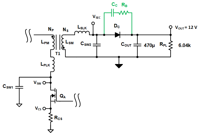 Figure 9-2 Simplified Flyback Schematic with Parasitic.
 To give an example of how to implement a snubber circuit, a 12 V, 10 W flyback design was created and simulated. The waveforms from this circuit are presented in Figure 9-2 and would trigger an OVP fault incorrectly due to ringing on the secondary winding (VSEC) through the transformer to VAUX.
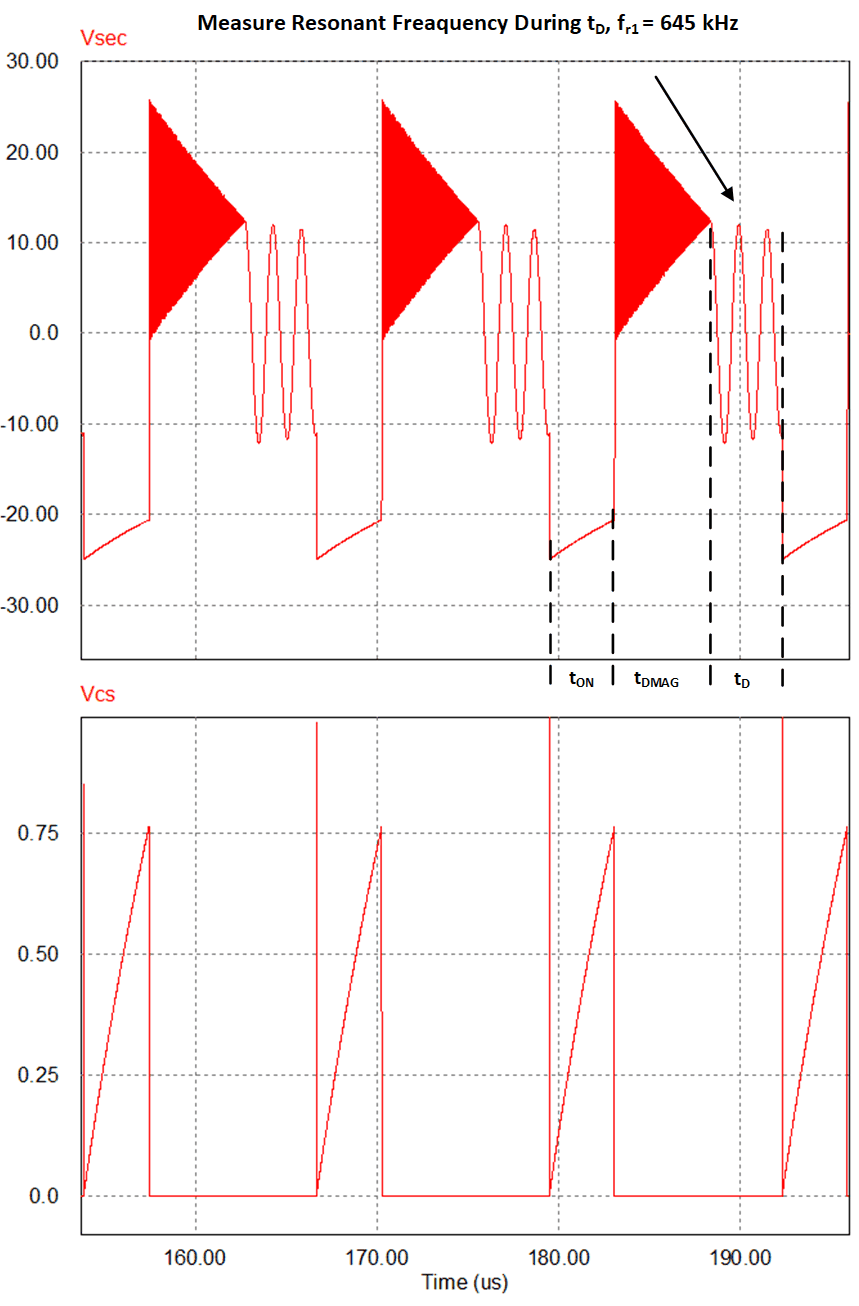 Figure 9-3 Measuring
Low Frequency Ringing to Calculate CSW2
To setup the snubber requires knowing or calculating the transformer’s primary ( LPM) and secondary LSM magnetizing induct, LSLK, CSW2. With this information the secondary magnetizing inductance (LSM) can be calculated by knowing the transformer primary to secondary turns ratio (NP/NS) and primary magnetizing inductance (LPM) which are given in the transformer data sheet and using equations Equation 16 and Equation 17. For this example the transformer had an LPM of 680 µH and NP/NS of 5.8. LSM for this design was calculated to be 20 µH.
To calculate CSW2 requires knowing LSM and studying the VSEC waveform and measuring the low frequency ringing (fr1) during the tD time interval, Figure 9-3. fr1 should be measured when the flyback converter is operating at light load and operating deep into DCM. In this example fr1 was measured to be 645 kHz. CSW2 can then be calculated using Equation 19, which for this example was 3 nF
The next step is to measure the high frequency ringing (fr2). during time interval tDMAG, Figure 9-4. This resonant frequency is caused by the interaction of CSW2 and LSECP. Based on fr2 and CSW2, LSECP can be calculated using Equation 21. With a measured fr2 of 14 MHz and CSW2 of 3 nF the calculated LSECP is approximately 43 nH.
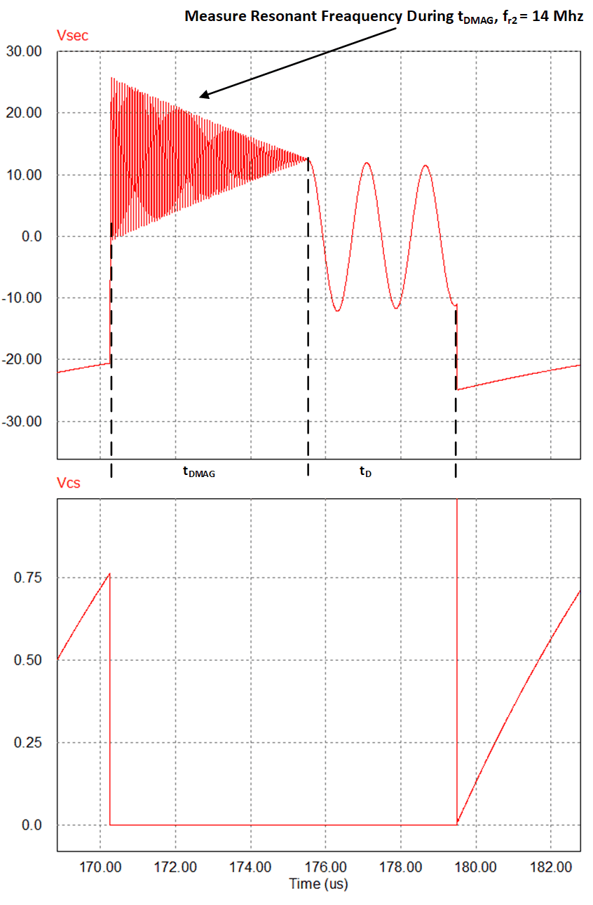 Figure 9-4 Measure
High Frequency Ringing During Time Interval tDMAG
Figure 9-4 Measure
High Frequency Ringing During Time Interval tDMAGSnubbing resistor RB is chosen to critically dampen the high-frequency ringing and can be calculated using Equation 22.
A standard resistor was chosen for resistor RB :
RB = 3.83
The snubbing capacitor CC was chosen based on Equation 23, based on the converter's maximum nominal switching frequency (fSW). By setting CC this way the snubber will only be active for 1% of the switching period, keeping snubber losses to a minimum. The flyback design being evaluated had a fSW of 75 kHz.
A standard capacitance value for CC was chosen for the design:
CC = 6.8 nF
The snubber components that were selected for RB and RC were applied to the circuit presented in Figure 1-1 and Figure 9-2. The result was the secondary winding was critically damped. Please refer to Figure 9-5 for damped waveforms results.
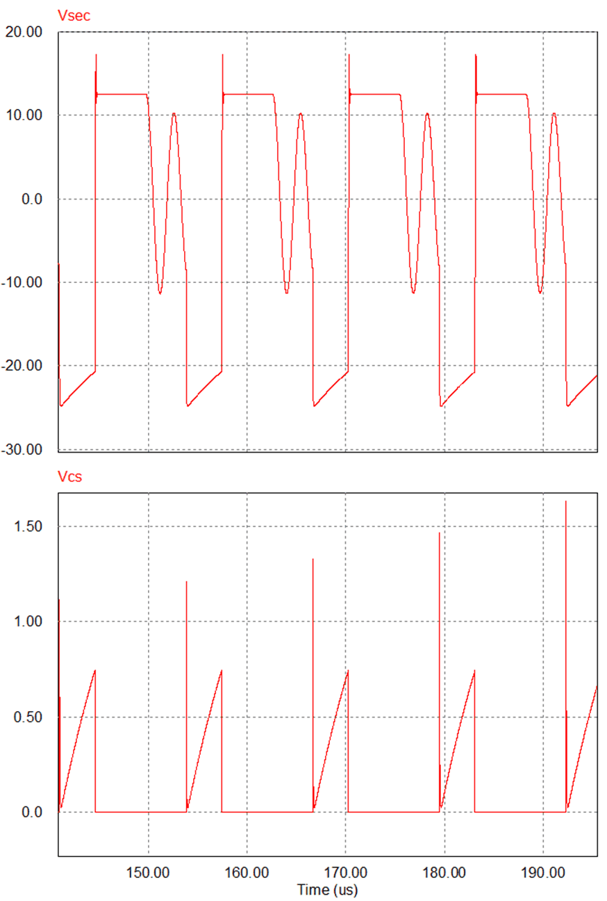 Figure 9-5 Snubber,
RB 3.83 ohms, CC = 6.8nF