SLLA475 December   2020 TCAN1144-Q1 , TCAN1146-Q1


  1. 1TCAN1144-Q1 and TCAN1146-Q1 Functional Safety Manual
  2. 2Trademarks
  3. 3Introduction
  4. 4TCAN114x-Q1 Hardware Component Functional Safety Capability
  5. 5Development Process for Management of Systematic Faults
    1. 5.1 TI New-Product Development Process
  6. 6TCAN1144-Q1 and TCAN1146-Q1 Component Overview
    1. 6.1 Targeted Applications
    2. 6.2 Hardware Component Functional Safety Concept
    3. 6.3 Functional Safety Constraints and Assumptions
  7. 7Description of Hardware Component Parts
    1. 7.1 CAN Transceiver
    2. 7.2 Digital Core
    3. 7.3 EEPROM
    4. 7.4 Power Control IP
      1. 7.4.1 Voltage Monitors
    5. 7.5 Thermal Shut Down
    6. 7.6 Digital Input/Outputs
  8. 8TCAN1144-Q1 and TCAN1146-Q1 Management of Random Faults
    1. 8.1 Fault Reporting
    2. 8.2 Functional Safety Mechanism Categories
    3. 8.3 Description of Functional Safety Mechanisms
      1. 8.3.1 CAN Communication
        1. 8.3.1.1 SM-1: CAN bus fault diagnostic
        2. 8.3.1.2 SM-2: Thermal shutdown; TSD
        3. 8.3.1.3 SM-3: CAN bus short circuit limiter, IOS
        4. 8.3.1.4 SM-4: CAN TXD pin dominant state timeout; tTXD_DTO
        5. 8.3.1.5 SM-17: CAN protocol
      2. 8.3.2 Supply Voltage Rail Monitoring
        1. 8.3.2.1 SM-5: VCC undervoltage; UVCC
        2. 8.3.2.2 SM-6: VSUP supply undervoltage; UVSUP
        3. 8.3.2.3 SM-7: VIO supply undervoltage; UVIO
      3. 8.3.3 SPI/Processor Communication
        1. 8.3.3.1 SM-8: Timout, Window or Q&A watchdog error - Normal mode
        2. 8.3.3.2 SM-9: SPI communication error; SPIERR
        3. 8.3.3.3 SM-10: Scratchpad write/read
        4. 8.3.3.4 SM-11: Sleep Wake Error Timer; tINACTIVE
      4. 8.3.4 Device Internal EEPROM
        1. 8.3.4.1 SM-12: Internal memory CRC; CRC_EEPROM
      5. 8.3.5 Floating Pins
        1. 8.3.5.1 SM-13: SCLK internal pull-up to VIO
        2. 8.3.5.2 SM-14: SDI internal pull-up to VIO
        3. 8.3.5.3 SM-15: nCS internal pull-up to VIO
        4. 8.3.5.4 SM-16: TXD internal pull-up to VIO
          1.        B Revision History

SM-11: Sleep Wake Error Timer; tINACTIVE

The sleep wake error (SWE) timer is a timer used to determine if specific external and internal functions are working. Upon power up, POR or UVSUP event, the SWE timer starts, tINACTIVE, and the processor has typically 4.5 minutes to configure the device, clear the PWRON flag or change the device to normal or listen mode. This feature cannot be disabled for power up. If the device has not had the PWRON flag cleared or been placed into normal or listen mode, it enters sleep mode. The SWE timer can be disabled for the other scenarios that cause the device to enter fail-safe mode by setting SWE_DIS; 8'h1C[7] = 1 and FS_DIS at 8'h17[0] = 1.

The device wakes up if the CAN bus provides a WUP or a local wake event takes place thus entering standby mode. Once in standby mode, the tSILENCE and tINACTIVE timers start. If the tINACTIVE expires the device re-enters sleep mode. When the device receives a CANINT, and LWU or FRAME_OVF such that the device leaves sleep mode and enters standby mode, the processor has tINACTIVE to clear the flags and place it into normal mode. If this does not happen, the device enters sleep mode. When in standby, normal or listen mode and the CANSLNT flag persists for tINACTIVE, the device enters sleep mode. Examples of events that could create this are the processor is no longer working and not able to exercise the SPI bus, or a go to sleep command comes in and the processor is not able to receive it or is not able to respond. See data sheet.

When fail-safe mode (FSM) is enabled and the SWE timer expires the device will enter FSM and will indicate the fault at 8'h50[7], 8'h50[4] and 8'h53[5] = FSM.

Figure 8-3 shows when the SWE timer, tINACTIVE, starts and what mode transitions take place.
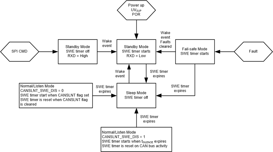
GUID-20201028-CA0I-VLBL-42WR-DG5WSWVSCC7Q-low.gifFigure 8-3 Sleep Wake Error (SWE) Timer, tINACTIVE