SLAA654A November 2014 – July 2015 CC430F6147 , MSP430F412 , MSP430F413 , MSP430F4132 , MSP430F415 , MSP430F4152 , MSP430F417 , MSP430F423A , MSP430F4250 , MSP430F425A , MSP430F4260 , MSP430F4270 , MSP430F427A , MSP430F435 , MSP430F4351 , MSP430F436 , MSP430F4361 , MSP430F437 , MSP430F4371 , MSP430F438 , MSP430F439 , MSP430F447 , MSP430F448 , MSP430F4481 , MSP430F449 , MSP430F4491 , MSP430F4616 , MSP430F46161 , MSP430F4617 , MSP430F46171 , MSP430F4618 , MSP430F46181 , MSP430F4619 , MSP430F46191 , MSP430F47126 , MSP430F47127 , MSP430F47163 , MSP430F47166 , MSP430F47167 , MSP430F47173 , MSP430F47176 , MSP430F47177 , MSP430F47183 , MSP430F47186 , MSP430F47187 , MSP430F47193 , MSP430F47196 , MSP430F47197 , MSP430F477 , MSP430F478 , MSP430F4783 , MSP430F4784 , MSP430F479 , MSP430F4793 , MSP430F4794 , MSP430F6433 , MSP430F6435 , MSP430F6436 , MSP430F6438 , MSP430F6458 , MSP430F6459 , MSP430F6630 , MSP430F6631 , MSP430F6632 , MSP430F6633 , MSP430F6634 , MSP430F6635 , MSP430F6636 , MSP430F6637 , MSP430F6638 , MSP430F6658 , MSP430F6659 , MSP430F6720 , MSP430F6720A , MSP430F6721 , MSP430F6721A , MSP430F6723 , MSP430F6723A , MSP430F6724 , MSP430F6724A , MSP430F6725 , MSP430F6725A , MSP430F6726 , MSP430F6726A , MSP430F6730 , MSP430F6730A , MSP430F6731 , MSP430F6731A , MSP430F6733 , MSP430F6733A , MSP430F6734 , MSP430F6734A , MSP430F6735 , MSP430F6735A , MSP430F6736 , MSP430F6736A , MSP430F6745 , MSP430F67451 , MSP430F67451A , MSP430F6745A , MSP430F6746 , MSP430F67461 , MSP430F67461A , MSP430F6746A , MSP430F6747 , MSP430F67471 , MSP430F67471A , MSP430F6747A , MSP430F6748 , MSP430F67481 , MSP430F67481A , MSP430F6748A , MSP430F6749 , MSP430F67491 , MSP430F67491A , MSP430F6749A , MSP430F67621 , MSP430F67621A , MSP430F67641 , MSP430F67641A , MSP430F6765 , MSP430F67651 , MSP430F67651A , MSP430F6765A , MSP430F6766 , MSP430F67661 , MSP430F67661A , MSP430F6766A , MSP430F6767 , MSP430F67671 , MSP430F67671A , MSP430F6767A , MSP430F6768 , MSP430F67681 , MSP430F67681A , MSP430F6768A , MSP430F6769 , MSP430F67691 , MSP430F67691A , MSP430F6769A , MSP430F6775 , MSP430F67751 , MSP430F67751A , MSP430F6775A , MSP430F6776 , MSP430F67761 , MSP430F67761A , MSP430F6776A , MSP430F6777 , MSP430F67771 , MSP430F67771A , MSP430F6777A , MSP430F6778 , MSP430F67781 , MSP430F67781A , MSP430F6778A , MSP430F6779 , MSP430F67791 , MSP430F67791A , MSP430F6779A , MSP430FE423 , MSP430FE4232 , MSP430FE423A , MSP430FE4242 , MSP430FE425 , MSP430FE4252 , MSP430FE425A , MSP430FE427 , MSP430FE4272 , MSP430FE427A , MSP430FG4250 , MSP430FG4260 , MSP430FG4270 , MSP430FG437 , MSP430FG438 , MSP430FG439 , MSP430FG4616 , MSP430FG4617 , MSP430FG4618 , MSP430FG4619 , MSP430FG477 , MSP430FG478 , MSP430FG479 , MSP430FG6425 , MSP430FG6426 , MSP430FG6625 , MSP430FG6626 , MSP430FR4131 , MSP430FR4132 , MSP430FR4133 , MSP430FR5870 , MSP430FR5872 , MSP430FR58721 , MSP430FR5922 , MSP430FR59221 , MSP430FR5970 , MSP430FR5972 , MSP430FR59721 , MSP430FR6820 , MSP430FR6822 , MSP430FR68221 , MSP430FR6870 , MSP430FR6872 , MSP430FR68721 , MSP430FR6877 , MSP430FR6879 , MSP430FR68791 , MSP430FR6887 , MSP430FR6888 , MSP430FR6889 , MSP430FR68891 , MSP430FR6920 , MSP430FR6922 , MSP430FR69221 , MSP430FR6927 , MSP430FR69271 , MSP430FR6928 , MSP430FR6970 , MSP430FR6972 , MSP430FR69721 , MSP430FR6977 , MSP430FR6979 , MSP430FR69791 , MSP430FR6987 , MSP430FR6988 , MSP430FR6989 , MSP430FR69891 , MSP430FW423 , MSP430FW425 , MSP430FW427 , MSP430FW428 , MSP430FW429
- Designing With MSP430™ MCUs and Segment LCDs
- Revision History
4.9 Ultra-Low-Power Features
MSP430 LCD modules are designed with ultra-low power as a key feature. In addition to some of the low power options discussed in the earlier sections (such as the adjustable charge pump voltage level, and options for external biasing), the charge pump is also only turned on for a small percentage of the overall operation of the module. It runs with a low duty cycle so that its peak current is only seen for a very small portion of the overall time that the LCD is on, helping the LCD to keep a very low overall average current.
The peak charge pump current can be found in the data sheet for the particular device being used. There is also usually a spec for the time to charge the CLCD charge pump cap when it is discharged, so this can help determine an average current for the LCD module – worst case the charge pump is at the peak current ICC,Peak,CP for the time tLCD,CP,on when CLCD has been discharged. The rest of the time, the module is in a much lower current state. In addition, using a low-leakage capacitor for CLCD can also help to reduce the energy consumption as it helps the charge pump run with a lower duty cycle.
 Figure 11. Low Charge Pump Duty Cycle
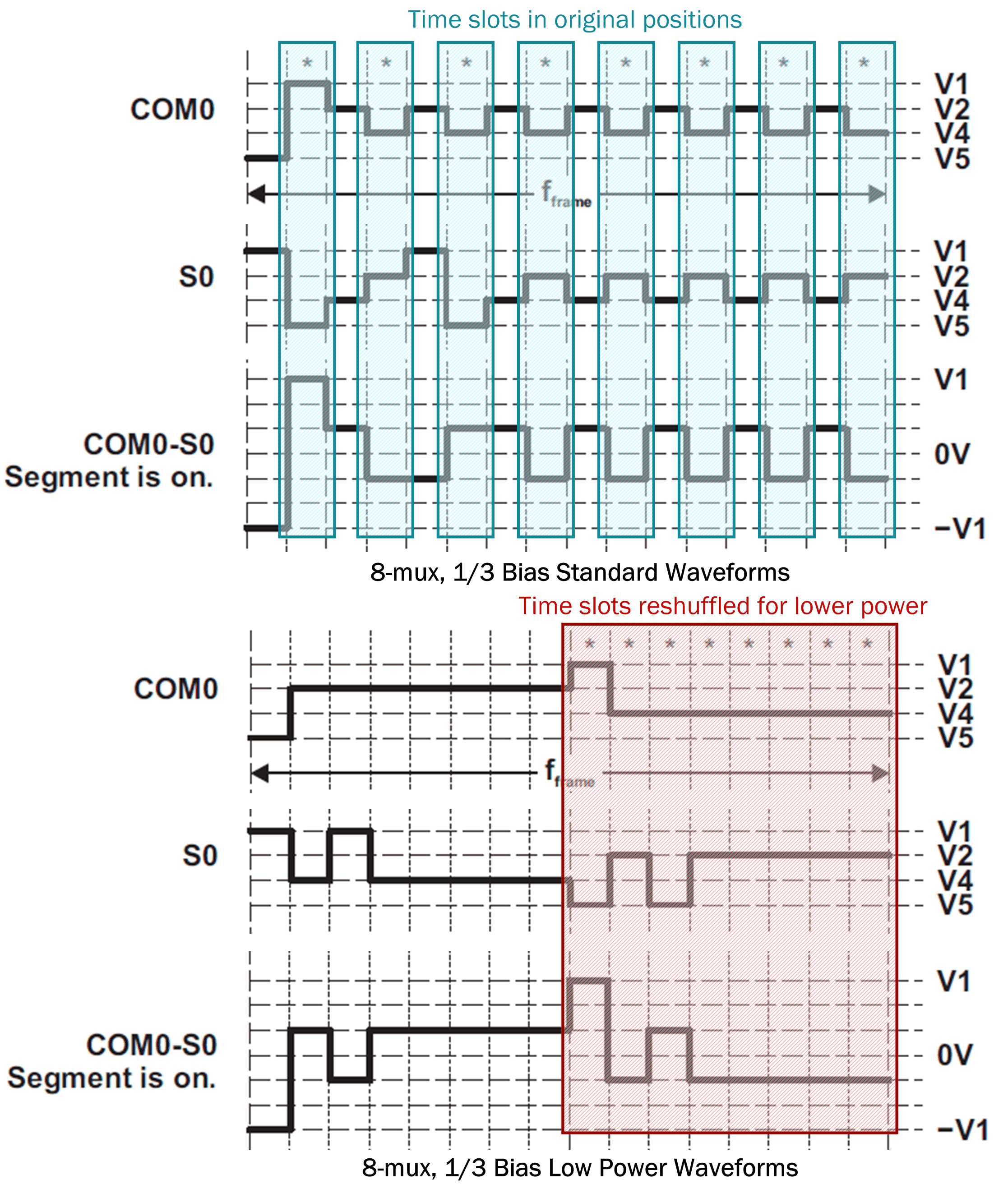
 MSP430 devices with LCD_C or LCD_E modules also have a setting for using lower power versions of the LCD waveforms. The lower power versions of the waveforms have the voltage sequence re-shuffled such that certain timeslots are grouped together. This makes for fewer switching events on each pin and lower current consumption. Figure 12 shows an example of the normal and lower power versions of waveforms for 8-mux mode.
 Figure 12. Low-Power Waveforms Example
 The LCD_E module is currently the lowest power LCD module in the MSP430 portfolio and is designed to be even lower power than the other MSP430 LCD devices. One key feature is that the module can remain operational and keep the LCD on all the way down to LPM3.5 mode, allowing for a new level of ultra-low power and enabling new LCD applications where the power supply is very limited. See the device-specific data sheet and user's guide for more details about LCD current consumption and LPM3.5 mode.