SBOA443 March 2021 INA293
2.3 Sample Rate
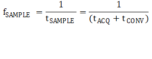
While not as vitally important as acquisition time or resolution, a third important parameter that merits discussion here is sample rate. Sample rate is the effective throughput of the device in terms of digitized samples, and is often determined with various design goals in mind, such as Nyquist criterion, additional resolution from oversampling, or even power considerations. In general, the maximum sampling rate of a device can be determined by adding the conversion time and the acquisition time of the device and taking the inverse of this total time, or
An important factor here, although not true of all ADCs, is that while conversion time for an ADC is a fixed quantity, the acquisition time of many devices can be altered by relaxing the sampling clock of the device, effectively widening the sampling window. This is an important feature when attempting to directly drive the ADC with a lower bandwidth sensor, as it will allow the amplifier to optimize achievable throughput once a stable filter is designed.