SBOA443 March 2021 INA293
3 The ADC Charge Bucket Filter
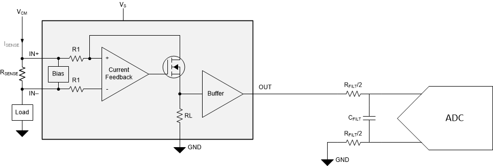
While it is possible for an amplifier to directly drive the inputs of an ADC by itself in certain situations, in most cases, a charge bucket filter is needed, connected as shown in Charge Bucket Filter, Single-Ended ADC with Ground Sense Configuration below.
 Figure 3-1 Charge Bucket Filter, Single-Ended ADC with Ground Sense Configuration
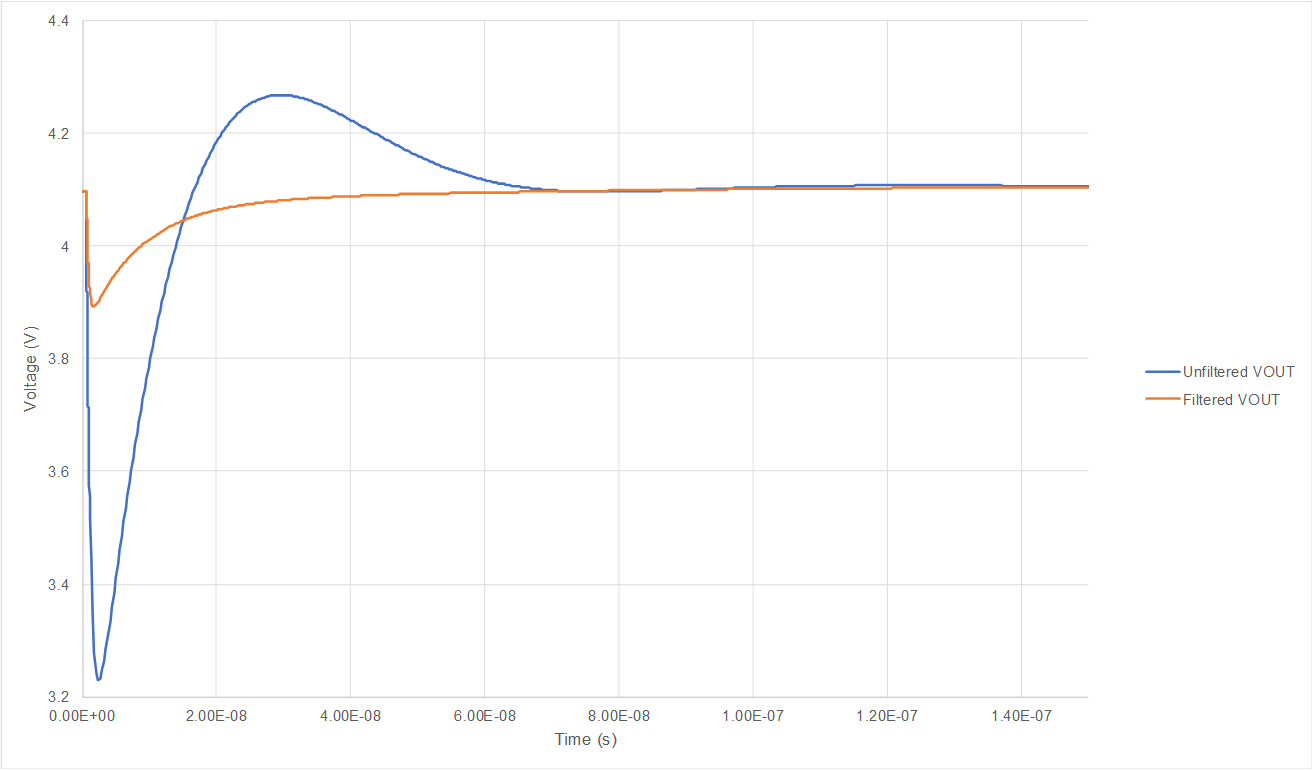
The purpose of this filter is not necessarily to provide anti-aliasing capabilities (although there may be potential to design to this), but rather to provide a bucket of additional energy to help charge the sample and hold node of the ADC to within 1/2 LSB inside of the acquisition window. This filter also helps to maintain stability in the system, as each sample in the sequence requires an inrush of charge, and often the amplifier cannot directly drive the input sampling structure for this requirement. In applications where this is possible, additional challenges such as spiking or droop on the signal can occur, and often require even higher bandwidths from the amplifier to properly recover, resulting in additional power needs from the amplifier, including higher quiescent current as a direct consequence of the higher bandwidth. An illustration of analog simulated outputs of both an unfiltered signal and a filtered signal are compared in Unfiltered vs. Filtered Output Signal.
 Figure 3-2 Unfiltered vs. Filtered Output Signal
As discussed in Math Behind R-C Component Selection, the following derivations and discussion are not found in textbook, but rather are approximations made based on assumptions from data over multiple designs. This approach combines the best aspects of multiple methods based on data, and provides an algorithm for circuit optimization. The assumptions made for the following analysis are:
- VIN = 100% FSR for worst case settling
- Total droop of the voltage allowed on the filter node (VFILT) is 100mV
- Error Target = 1/2 LSB
- Current Sense Amplifier is approximated as a second order system
- The Current Sense Amplifier is 4 times faster than the filter