SBOA443 March 2021 INA293
3.1 The Filter Capacitor, CFILT
Recall that for a capacitor, the charge stored is equal to the voltage present on the capacitor multiplied by the capacitance. Then, for the sample and hold capacitor internal to the ADC, it can be expressed that
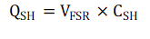
Using this expression, CSH is defined as the internal sample and hold capacitance value of the ADC, and VFSR as the maximum possible voltage of the full scale range across CSH. The corresponding Coulumb product then gives us the maximum possible Coulombs that CSH could need to charge to within a single acquisition cycle.
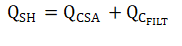
When the switch of the sample and hold structure closes, charge from the current sense amplifier as well as charge held on the filter capacitor both move to charge the sample and hold structure. It can threrefore be epxressed that
While the charge delivered by the amplifier comes from its output stage, charge from the filter capacitor is depleted, and causes the voltage on the node to droop. Here, the assumption is made that half of the charge needed to charge CSH is sourced from the filter capacitor. The general form of this equation is given as
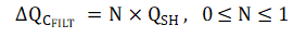
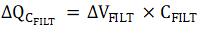
where here, N = 0.5. As the capacitance of the chosen filter capacitor is a fixed value, we can then attribute the change in charge to the droop in voltage as
Combining these expressions, and solving for CFILT, a final expression is derived of
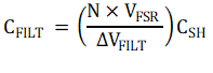
By the assumptions of VFSR = 4.096V ≅ 4V, and VDROOP = ΔVFILT = 100mV, the parenthetical term reduces to a coefficient that provides a sizing relationship for the filter capacitor of
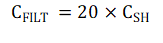
This implies that for the given sample and hold capacitance of an ADC operating at a full scale range of 4V, to maintain less than 100mV droop on the input node, a filter capacitor 20 times the size of sample and hold capacitance should be mounted, provided the amplifier is capable of supplying the remaining charge. If this is not the case, the droop may be greater than the assumed 100mV, which may or may not be acceptable based on system specifications.
A capacitor of this magnitude will often be difficult to implement, as amplifiers typically cannot drive large capacitive loads on their own and maintain stability. Current sense amplifiers are no exception here, so ways to ensure stability will need to be examined to successfully drive this type of load.