SBAU361 December 2020
4.1.1 ADC35XX GUI: Bypass Mode Configuration
After power up, the ADC3664EVM is preconfigured for 14 bit, 2W Bypass Mode (No Decimation). There are other modes and sample rates that can be used in Bypass Mode, and Table 4-1 shows examples of required clocks for different serialization options (1W and 1/2W). To calculate the correct DCLKIN frequency for the desired sampling rate and mode, multiply the sampling rate by the DCLKIN multiplier (Serialization factor).
| Interface Mode | DCLKIN Multiplier (Serialization factor) |
Example Sample Clock | Required DCLKIN Frequency |
|---|---|---|---|
| 2 Wire | 3.5 | 125 MSPS | 437.5 MHz |
| 1 Wire | 7 | 65 MSPS | 455 MHz |
| 1/2 Wire | 14 | 35 MSPS | 490 MHz |
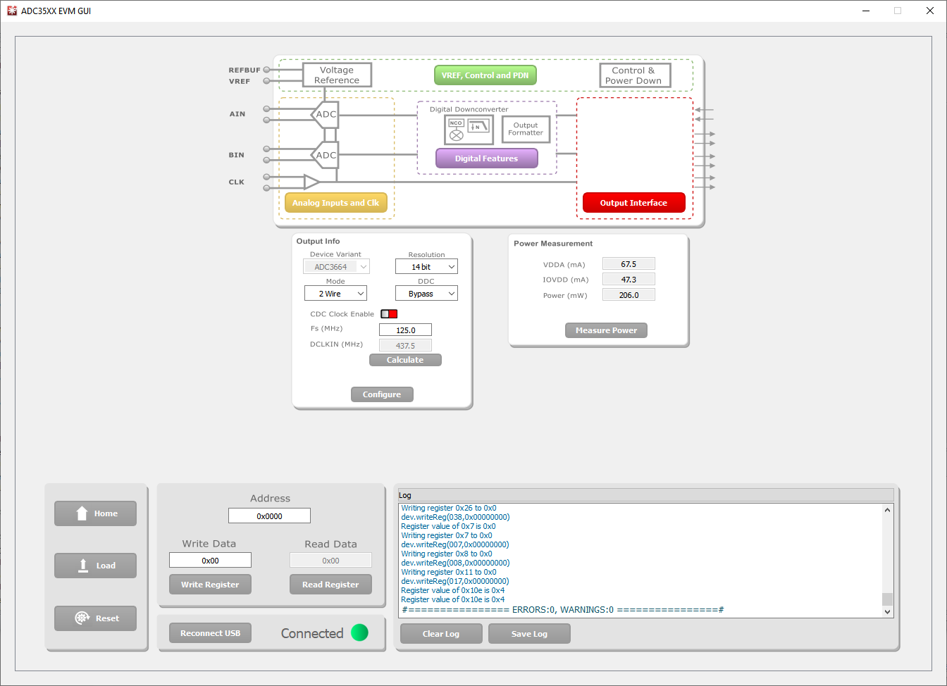
For this 14 bit, 2-Wire example, ensure that the sampling clock (J9) and DCLKIN (J7) are connected before launching the ADC35XX EVM GUI. In this example, the sampling clock is 125 MHz, and the DCLKIN is 437.5 MHz.
After launching the ADC35xx GUI, the below items should already be populated. If not, perform the following steps for 14 bit, 2W Bypass mode:
- Under Resolution, select "14 bit".
- Under Mode, select "2 Wire".
- Under DDC, select "Bypass".
- Enter "125M" for "Fs (MHz)".
- Ensure that "CDC Enable" is red (disabled).
- Click "Configure" button.
 Figure 4-1 ADC35XXEVM GUI: ADC3664EVM Bypass
Mode