SNLS375C June 1998 – January 2015 DS26C31T
PRODUCTION DATA.
- 1 Features
- 2 Applications
- 3 Description
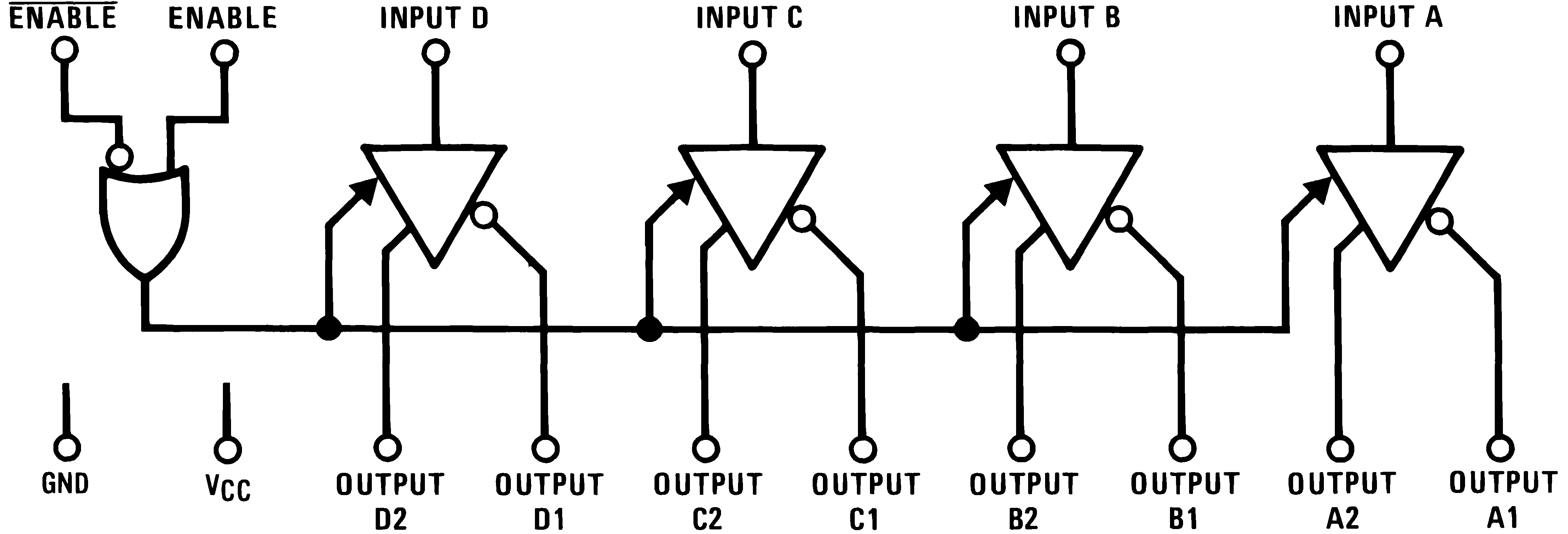
- 4 Device Logic Diagram
- 5 Revision History
- 6 Pin Configuration and Functions
- 7 Specifications
- 8 Parameter Measurement Information
- 9 Detailed Description
- 10Application and Implementation
- 11Power Supply Recommendations
- 12Layout
- 13Device and Documentation Support
- 14Mechanical, Packaging, and Orderable Information
1 Features
- TTL Input Compatible
- Typical Propagation Delays: 6 ns
- Typical Output Skew: 0.5 ns
- Outputs Will Not Load Line When VCC = 0 V
- DS26C31T Meets the Requirements of EIA Standard RS-422
- Operation From Single 5-V Supply
- Tri-State Outputs for Connection to System Buses
- Low Quiescent Current
- Available in Surface Mount
- Mil-Std-883C Compliant
2 Applications
Differential Line Driver for RS-422 Applications
3 Description
The DS26C31 device is a quad differential line driver designed for digital data transmission over balanced lines. The DS26C31T meets all the requirements of EIA standard RS-422 while retaining the low power characteristics of CMOS. The DS26C31M is compatible with EIA standard RS-422; however, one exception in test methodology is taken(2). This enables the construction of serial and terminal interfaces while maintaining minimal power consumption.
The DS26C31 accepts TTL or CMOS input levels and translates these to RS-422 output levels. This part uses special output circuitry that enables the drivers to power down without loading down the bus. This device has enable and disable circuitry common to all four drivers. The DS26C31 is pin compatible to the AM26LS31 and the DS26LS31.
All inputs are protected against damage due to electrostatic discharge by diodes to VCC and ground.
Device Information(1)
| PART NUMBER | PACKAGE | BODY SIZE (NOM) |
|---|---|---|
| DS26C31M | SNLS3759577 | 9.90 mm × 3.91 mm |
| PDIP (16) | 19.304 mm × 6.35 mm | |
| DS26C31T | SNLS3759577 | 9.90 mm × 3.91 mm |
| PDIP (16) | 19.304 mm × 6.35 mm |
- For all available packages, see the orderable addendum at the end of the datasheet.
- The DS26C31M (−55°C to 125°C) is tested with VOUT between 6 V and 0 V while RS-422A condition is 6 V and −0.25 V.
4 Device Logic Diagram