SNLS375C June 1998 – January 2015 DS26C31T
PRODUCTION DATA.
- 1 Features
- 2 Applications
- 3 Description
- 4 Device Logic Diagram
- 5 Revision History
- 6 Pin Configuration and Functions
- 7 Specifications
- 8 Parameter Measurement Information
- 9 Detailed Description
- 10Application and Implementation
- 11Power Supply Recommendations
- 12Layout
- 13Device and Documentation Support
- 14Mechanical, Packaging, and Orderable Information
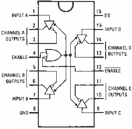
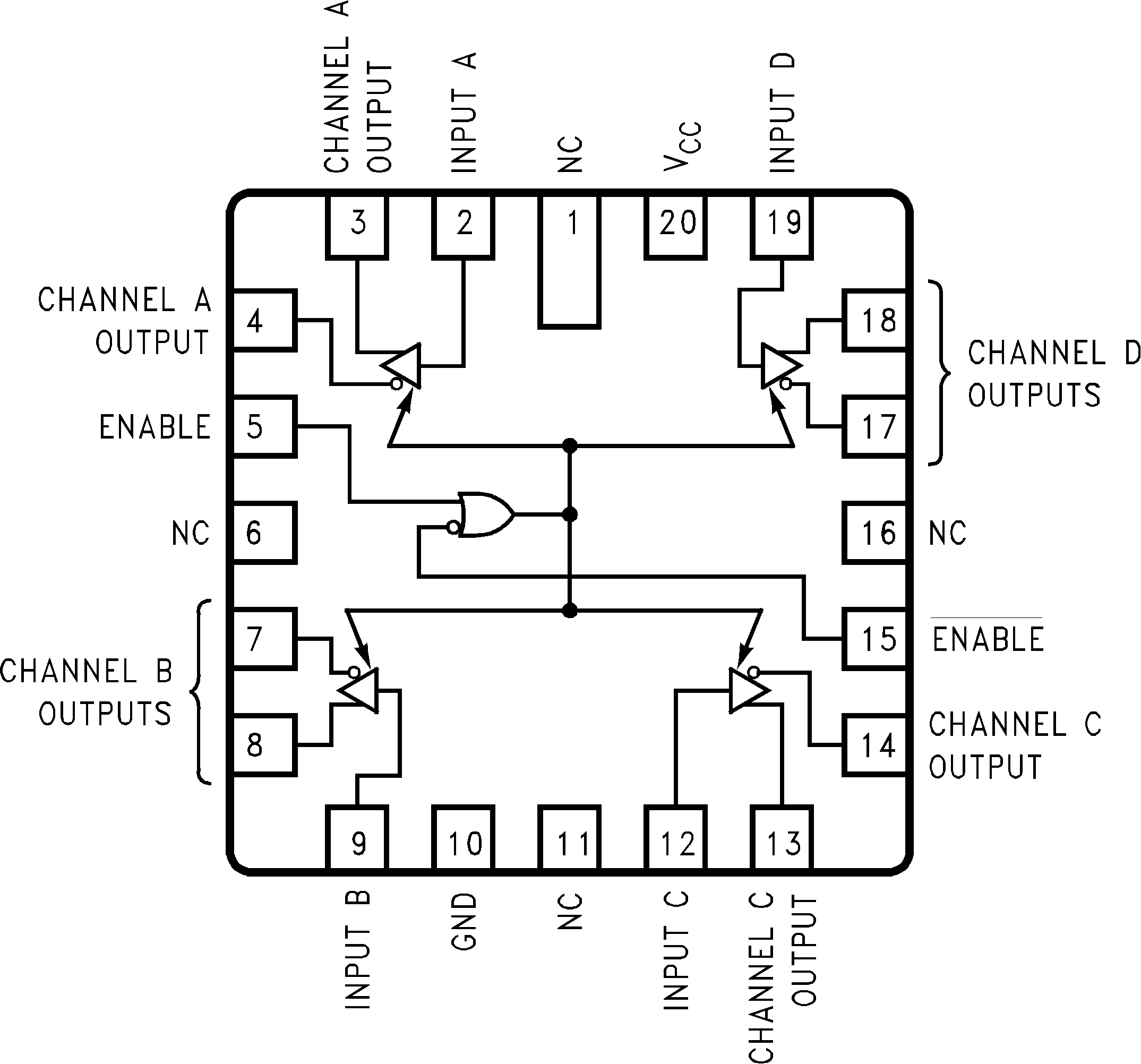
6 Pin Configuration and Functions
D, NFG Package
16 Pins
Top View
NAJ Package
20 Pins
Top View
Pin Functions
| PIN | I/O | DESCRIPTION | |
|---|---|---|---|
| NAME | NO.(1) | ||
| DIFFERENTIAL SIGNALING I/O | |||
| CHANNEL A OUTPUTS (–, +) | 3, 2 | O | Channel A inverting and non-inverting differential driver outputs |
| CHANNEL B OUTPUTS (–, +) | 5, 6 | O | Channel B inverting and non-inverting differential driver outputs |
| CHANNEL C OUTPUTS (–, +) | 11, 10 | O | Channel C inverting and non-inverting differential driver outputs |
| CHANNEL D OUTPUTS (–, +) | 13, 14 | O | Channel D inverting and non-inverting differential driver outputs |
| INPUT A | 1 | I | TTL/CMOS compatible input for channel A |
| INPUT B | 7 | I | TTL/CMOS compatible input for channel B |
| INPUT C | 9 | I | TTL/CMOS compatible input for channel C |
| INPUT D | 15 | I | TTL/CMOS compatible input for channel D |
| CONTROL PINS | |||
| ENABLE | 4 | I | Logic-high ENABLE Control |
| ENABLE | 12 | I | Logic-low ENABLE Control |
| POWER | |||
| GND | 8 | — | GND Pin |
| VCC | 16 | — | Supply pin, provide 5 V supply |
(1) Pin numbers correspond to PDIP and SOIC packages.