SNLS375C June 1998 – January 2015 DS26C31T
PRODUCTION DATA.
- 1 Features
- 2 Applications
- 3 Description
- 4 Device Logic Diagram
- 5 Revision History
- 6 Pin Configuration and Functions
- 7 Specifications
- 8 Parameter Measurement Information
- 9 Detailed Description
- 10Application and Implementation
- 11Power Supply Recommendations
- 12Layout
- 13Device and Documentation Support
- 14Mechanical, Packaging, and Orderable Information
10 Application and Implementation
NOTE
Information in the following applications sections is not part of the TI component specification, and TI does not warrant its accuracy or completeness. TI’s customers are responsible for determining suitability of components for their purposes. Customers should validate and test their design implementation to confirm system functionality.
10.1 Application Information
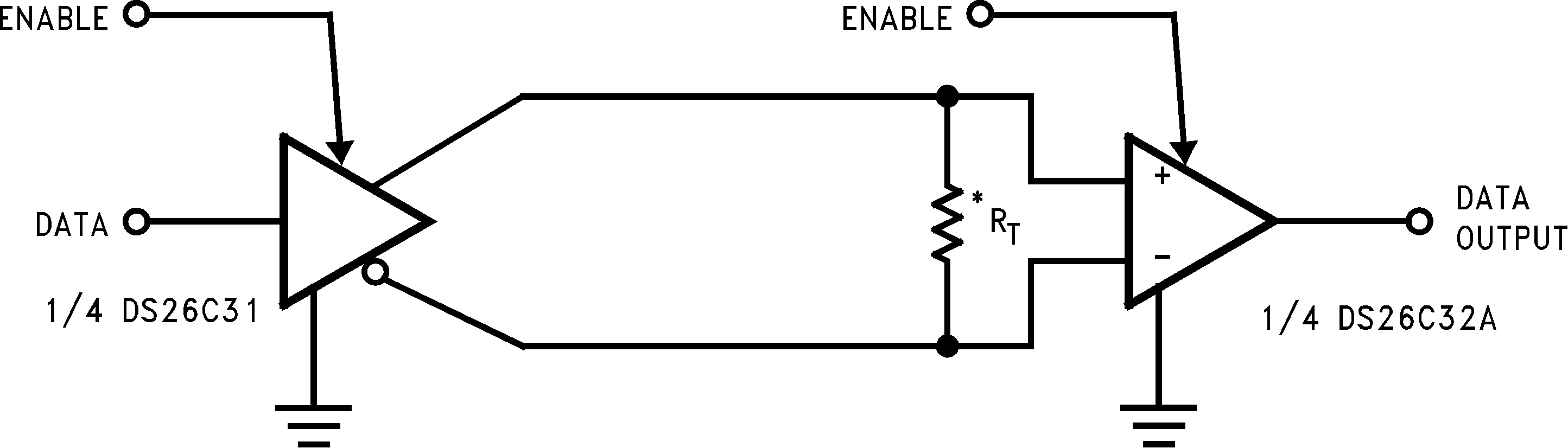
The DS26C31 is a quad differential line driver designed for applications that require long distance digital data transmission over balanced cables. The DS26C31 can be used in applications that require conversion from TTL or CMOS input levels to differential signal levels, compatible to RS-422. The use of complimentary signaling in a balanced transmission media provides good immunity in the midst of noisy environments or shifts in ground reference potential.
10.2 Typical Application
Figure 28 depicts a typical implementation of the DS26C31x device in a RS-422 application.
10.2.1 Design Requirements
- Apply TTL or LVCMOS signal to driver input lines INPUT A-D.
- Transmit complementary outputs at OUTPUT A-D.
- Use controlled-impedance transmission lines such as printed circuit board traces, twisted-pair wires or parallel wire cable.
- Place a terminating resistor at the far end of the differential pair.
10.2.2 Detailed Design Procedure
- Connect VCC and GND pins to the power and ground planes of the PCB with a 0.1-µF bypass capacitor.
- Use TTL/LVCMOS logic levels at INPUT A-D.
- Use controlled-impedance transmission media for the differential output signals.
- Place an optional terminating resistor at the far-end of the differential pair to avoid reflection.
10.2.3 Application Curves
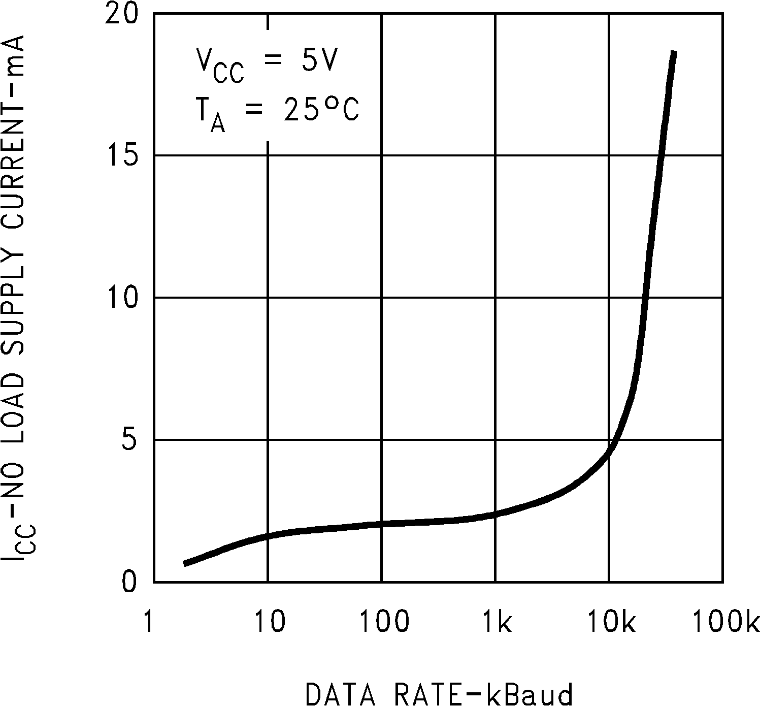 Figure 29. No Load Supply Current vs Data Rate
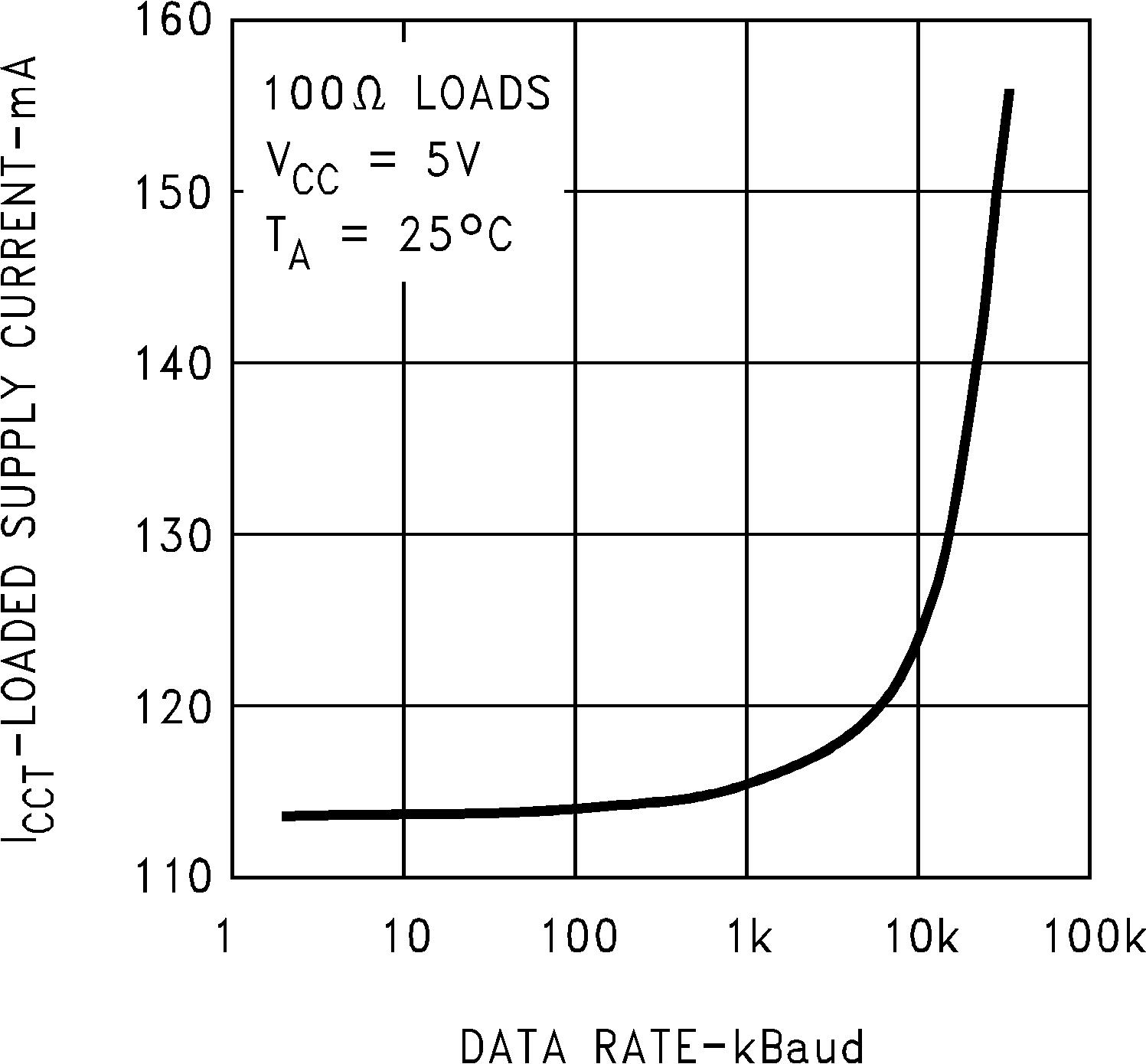 Figure 30. Loaded Supply Current vs Data Rate