SNLS375C June 1998 – January 2015 DS26C31T
PRODUCTION DATA.
- 1 Features
- 2 Applications
- 3 Description
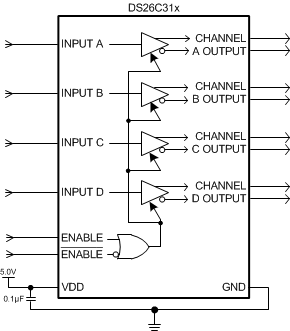
- 4 Device Logic Diagram
- 5 Revision History
- 6 Pin Configuration and Functions
- 7 Specifications
- 8 Parameter Measurement Information
- 9 Detailed Description
- 10Application and Implementation
- 11Power Supply Recommendations
- 12Layout
- 13Device and Documentation Support
- 14Mechanical, Packaging, and Orderable Information
9 Detailed Description
9.1 Overview
The DS26C31 is a quad differential line driver designed for data transmission over balanced cable or printed circuit board traces. The DS26C31M supports a temperature range of -55°C to 125°C, while the DS26C31T supports a temperature range of -40°C to 85°C.
9.2 Functional Block Diagram
9.3 Feature Description
Each driver converts the TTL or CMOS signal at its input to a pair of complementary differential outputs. The drivers are enabled when the ENABLE control pin is a logic HIGH or when the ENABLE control pin is a logic LOW.
9.4 Device Functional Modes
Table 1. Function Table(1)
| ENABLE | ENABLE | INPUT | NON-INVERTING OUTPUT | INVERTING OUTPUT |
|---|---|---|---|---|
| L | H | X | Z | Z |
| All other combinations of enable inputs | L | L | H | |
| H | H | L | ||
(1) L = Low logic state
X = Irrelevant
H = High logic state
Z = Tri-state (high impedance)
X = Irrelevant
H = High logic state
Z = Tri-state (high impedance)