SNLS375C June 1998 – January 2015 DS26C31T
PRODUCTION DATA.
- 1 Features
- 2 Applications
- 3 Description
- 4 Device Logic Diagram
- 5 Revision History
- 6 Pin Configuration and Functions
- 7 Specifications
- 8 Parameter Measurement Information
- 9 Detailed Description
- 10Application and Implementation
- 11Power Supply Recommendations
- 12Layout
- 13Device and Documentation Support
- 14Mechanical, Packaging, and Orderable Information
7 Specifications
7.1 Absolute Maximum Ratings(1)(2)(3)
| MIN | MAX | UNIT | ||
|---|---|---|---|---|
| Supply Voltage (VCC) | −0.5 | 7 | V | |
| DC Input Voltage (VIN) | −1.5 | VCC +1.5 | V | |
| DC Output Voltage (VOUT) | −0.5 | 7 | V | |
| Clamp Diode Current (IIK, IOK) | –20 | 20 | mA | |
| DC Output Current, per pin (IOUT) | –150 | 150 | mA | |
| DC VCC or GND Current, per pin (ICC) | ||||
| Max Power Dissipation (PD) at 25°C(4) | Ceramic “NFE” package | 2419 | mW | |
| Plastic “NFG” package | 1736 | mW | ||
| SOIC “D” package | 1226 | mW | ||
| Ceramic “NAD” package | 1182 | mW | ||
| Ceramic “NAJ” package | 2134 | mW | ||
| Lead Temperature (TL) | (Soldering, 4 s) | 260 | °C | |
| Storage Temperature, Tstg | −65 | 150 | °C | |
(1) Stresses beyond those listed under Absolute Maximum Ratings may cause permanent damage to the device. These are stress ratings only, which do not imply functional operation of the device at these or any other conditions beyond those indicated under Recommended Operating Conditions. Exposure to absolute-maximum-rated conditions for extended periods may affect device reliability.
(2) Unless otherwise specified, all voltages are referenced to ground. All currents into device pins are positive, all currents out of device pins are negative.
(3) If Military/Aerospace specified devices are required, please contact the Texas Instruments Sales Office/ Distributors for availability and specifications.
(4) Ratings apply to ambient temperature at 25°C. Above this temperature derate NFG package at 13.89 mW/°C, NFE package 16.13 mW/°C, D package 9.80 mW/°C, NAJ package 12.20 mW/°C, and NAD package 6.75 mW/°C.
7.2 Recommended Operating Conditions
| MIN | MAX | UNIT | ||
|---|---|---|---|---|
| Supply Voltage (VCC) | 4.50 | 5.50 | V | |
| DC Input or Output Voltage | (VIN, VOUT) | 0 | VCC | V |
| Operating Temperature Range (TA) | DS26C31T | −40 | 85 | °C |
| DS26C31M | −55 | 125 | °C | |
| Input Rise or Fall Times (tr, tf) | 500 | ns | ||
7.3 DC Electrical Characteristics
VCC = 5 V ± 10% (unless otherwise specified)(1)| PARAMETER | TEST CONDITIONS | MIN | TYP | MAX | UNIT | ||
|---|---|---|---|---|---|---|---|
| VIH | High Level Input Voltage | 2.0 | V | ||||
| VIL | Low Level Input Voltage | 0.8 | V | ||||
| VOH | High Level Output Voltage | VIN = VIH or VIL, | 2.5 | 3.4 | V | ||
| IOUT = −20 mA | |||||||
| VOL | Low Level Output Voltage | VIN = VIH or VIL, | 0.3 | 0.5 | V | ||
| IOUT = 20 mA | |||||||
| VT | Differential Output Voltage | RL = 100 Ω | 2.0 | 3.1 | V | ||
| See(2) | |||||||
| |VT| − |VT | | Difference In Differential Output | RL = 100 Ω | 0.4 | V | |||
| See(2) | |||||||
| VOS | Common Mode Output Voltage | RL = 100 Ω | 1.8 | 3.0 | V | ||
| See(2) | |||||||
| |VOS − VOS | | Difference In Common Mode Output | RL = 100 Ω | 0.4 | V | |||
| See(2) | |||||||
| IIN | Input Current | VIN = VCC, GND, VIH, or VIL | ±1.0 | μA | |||
| ICC | Quiescent Supply Current(3) | DS26C31T | VIN = VCC or GND | 200 | 500 | μA | |
| IOUT = 0 μA | VIN = 2.4 V or 0.5 V(3) | 0.8 | 2.0 | mA | |||
| DS26C31M | VIN = VCC or GND | 200 | 500 | μA | |||
| IOUT = 0 μA | VIN = 2.4 V or 0.5 V(3) | 0.8 | 2.1 | mA | |||
| IOZ | TRI-STATE Output Leakage Current | VOUT = VCC or GND | |||||
| ENABLE = VIL | ±0.5 | ±5.0 | μA | ||||
| ENABLE = VIH | |||||||
| ISC | Output Short Circuit Current | VIN = VCC or GND(2)(4) | −30 | −150 | mA | ||
| IOFF | Output Leakage Current Power Off(2) | DS26C31T | VOUT = 6 V | 100 | μA | ||
| VCC = 0 V | VOUT = −0.25 V | −100 | μA | ||||
| DS26C31M | VOUT = 6 V | 100 | μA | ||||
| VCC = 0 V | VOUT = 0 V(5) | −100 | μA | ||||
(1) Unless otherwise specified, min/max limits apply across the recommended operating temperature range. All typicals are given for VCC = 5 V and TA = 25°C.
(2) See EIA Specification RS-422 for exact test conditions.
(3) Measured per input. All other inputs at VCC or GND.
(4) This is the current sourced when a high output is shorted to ground. Only one output at a time should be shorted.
(5) The DS26C31M (−55°C to +125°C) is tested with VOUT between +6 V and 0 V while RS-422A condition is +6 V and −0.25 V.
7.4 Switching Characteristics
VCC = 5 V ±10%, tr ≤ 6 ns, tf ≤ 6 ns (Figure 22, Figure 23, Figure 24, Figure 25)(1)| PARAMETER | TEST CONDITIONS | MIN | TYP | DS26C31T | DS26C31M | UNIT | |
|---|---|---|---|---|---|---|---|
| MAX | MAX | ||||||
| tPLH, tPHL | Propagation Delays Input to Output | S1 Open | 2 | 6 | 11 | 14 | ns |
| Skew | (2) | S1 Open | 0.5 | 2.0 | 3.0 | ns | |
| tTLH, tTHL | Differential Output Rise And Fall Times | S1 Open | 6 | 10 | 14 | ns | |
| tPZH | Output Enable Time | S1 Closed | 11 | 19 | 22 | ns | |
| tPZL | Output Enable Time | S1 Closed | 13 | 21 | 28 | ns | |
| tPHZ | Output Disable Time(3) | S1 Closed | 5 | 9 | 12 | ns | |
| tPLZ | Output Disable Time(3) | S1 Closed | 7 | 11 | 14 | ns | |
| CPD | Power Dissipation Capacitance(4) | 50 | pF | ||||
| CIN | Input Capacitance | 6 | pF | ||||
(1) Unless otherwise specified, min/max limits apply across the recommended operating temperature range. All typicals are given for VCC = 5 V and TA = 25°C.
(2) Skew is defined as the difference in propagation delays between complementary outputs at the 50% point.
(3) Output disable time is the delay from ENABLE or ENABLE being switched to the output transistors turning off. The actual disable times are less than indicated due to the delay added by the RC time constant of the load.
(4) CPD determines the no load dynamic power consumption, PD = CPD VCC2 f + ICC VCC, and the no load dynamic current consumption, IS = CPD VCC f + ICC.
7.5 Comparison Table of Switching Characteristics into “LS-Type” Load
VCC = 5 V, TA = 25°C, tr ≤ 6 ns, tf ≤ 6 ns (Figure 23, Figure 25, Figure 26, Figure 27) (1)| PARAMETER | TEST CONDITIONS | DS26C31T | DS26LS31C | UNIT | |||
|---|---|---|---|---|---|---|---|
| TYP | MAX | TYP | MAX | ||||
| tPLH, tPHL | Propagation Delays Input to Output | CL = 30 pF | 6 | 8 | 10 | 15 | ns |
| S1 Closed | |||||||
| S2 Closed | |||||||
| Skew | See(2) | CL = 30 pF | 0.5 | 1.0 | 2.0 | 6.0 | ns |
| S1 Closed | |||||||
| S2 Closed | |||||||
| tTHL, tTLH | Differential Output Rise and Fall Times | CL = 30 pF | 4 | 6 | ns | ||
| S1 Closed | |||||||
| S2 Closed | |||||||
| tPLZ | Output Disable Time(3) | CL = 10 pF | 6 | 9 | 15 | 35 | ns |
| S1 Closed | |||||||
| S2 Open | |||||||
| tPHZ | Output Disable Time(3) | CL = 10 pF | 4 | 7 | 15 | 25 | ns |
| S1 Open | |||||||
| S2 Closed | |||||||
| tPZL | Output Enable Time | CL = 30 pF | 14 | 20 | 20 | 30 | ns |
| S1 Closed | |||||||
| S2 Open | |||||||
| tPZH | Output Enable Time | CL = 30 pF | 11 | 17 | 20 | 30 | ns |
| S1 Open | |||||||
| S2 Closed | |||||||
(1) This table is provided for comparison purposes only. The values in this table for the DS26C31 reflect the performance of the device but are not tested or verified.
(2) Skew is defined as the difference in propagation delays between complementary outputs at the 50% point.
(3) Output disable time is the delay from ENABLE or ENABLE being switched to the output transistors turning off. The actual disable times are less than indicated due to the delay added by the RC time constant of the load.
7.6 Typical Characteristics
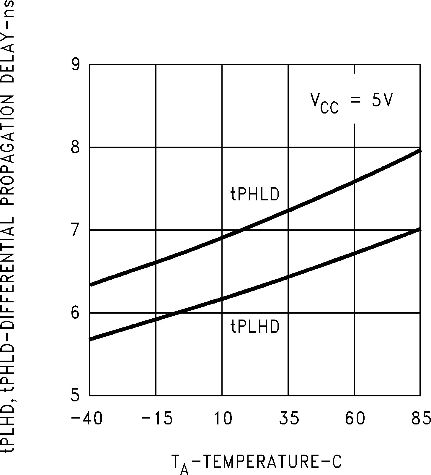 Figure 1. Differential Propagation Delay vs Temperature
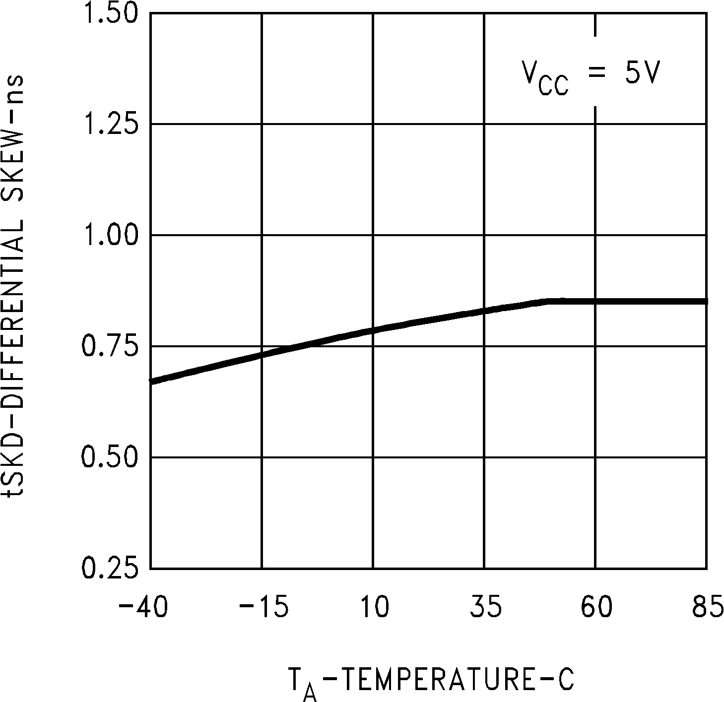 Figure 3. Differential Skew vs Temperature
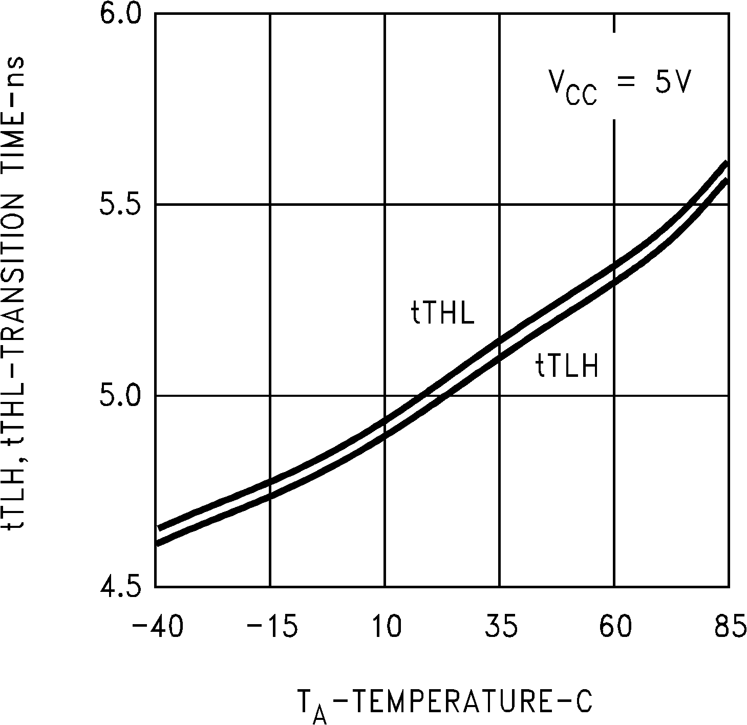 Figure 5. Differential Transition Time vs Temperature
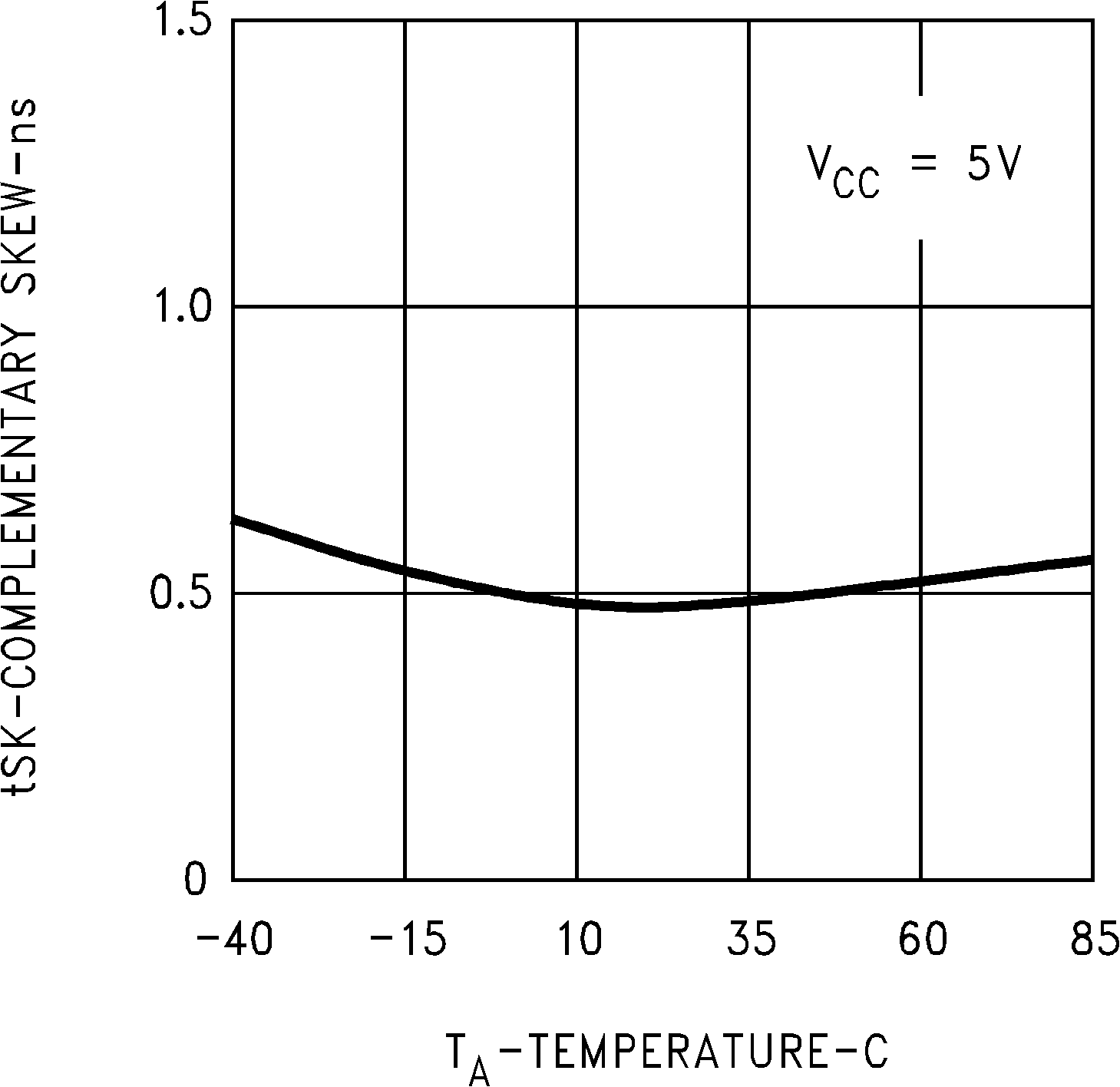 Figure 7. Complementary Skew vs Temperature
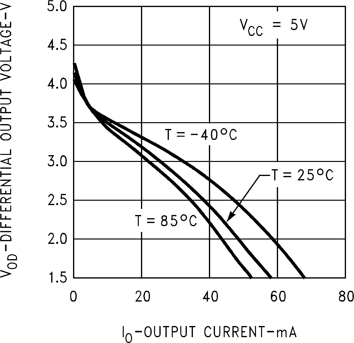 Figure 9. Differential Output Voltage vs Output Current
 Figure 11. Output High Voltage vs Output High Current
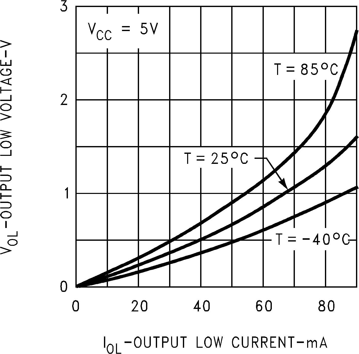 Figure 13. Output Low Voltage vs Output Low Current
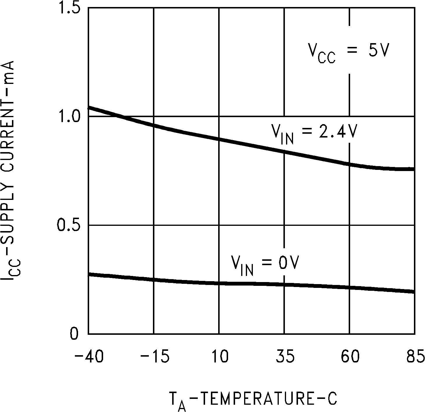 Figure 15. Supply Current vs Temperature
 Figure 17. Output Low Voltage vs Output Low Current
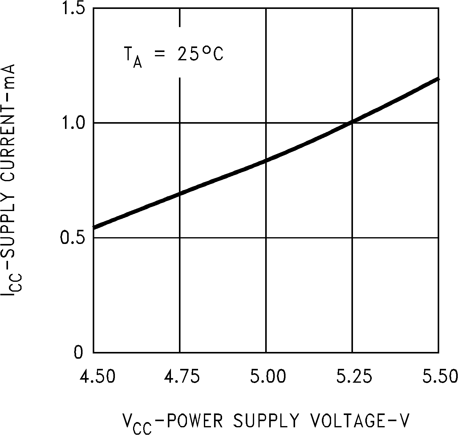 Figure 19. Supply Current vs Power Supply Voltage
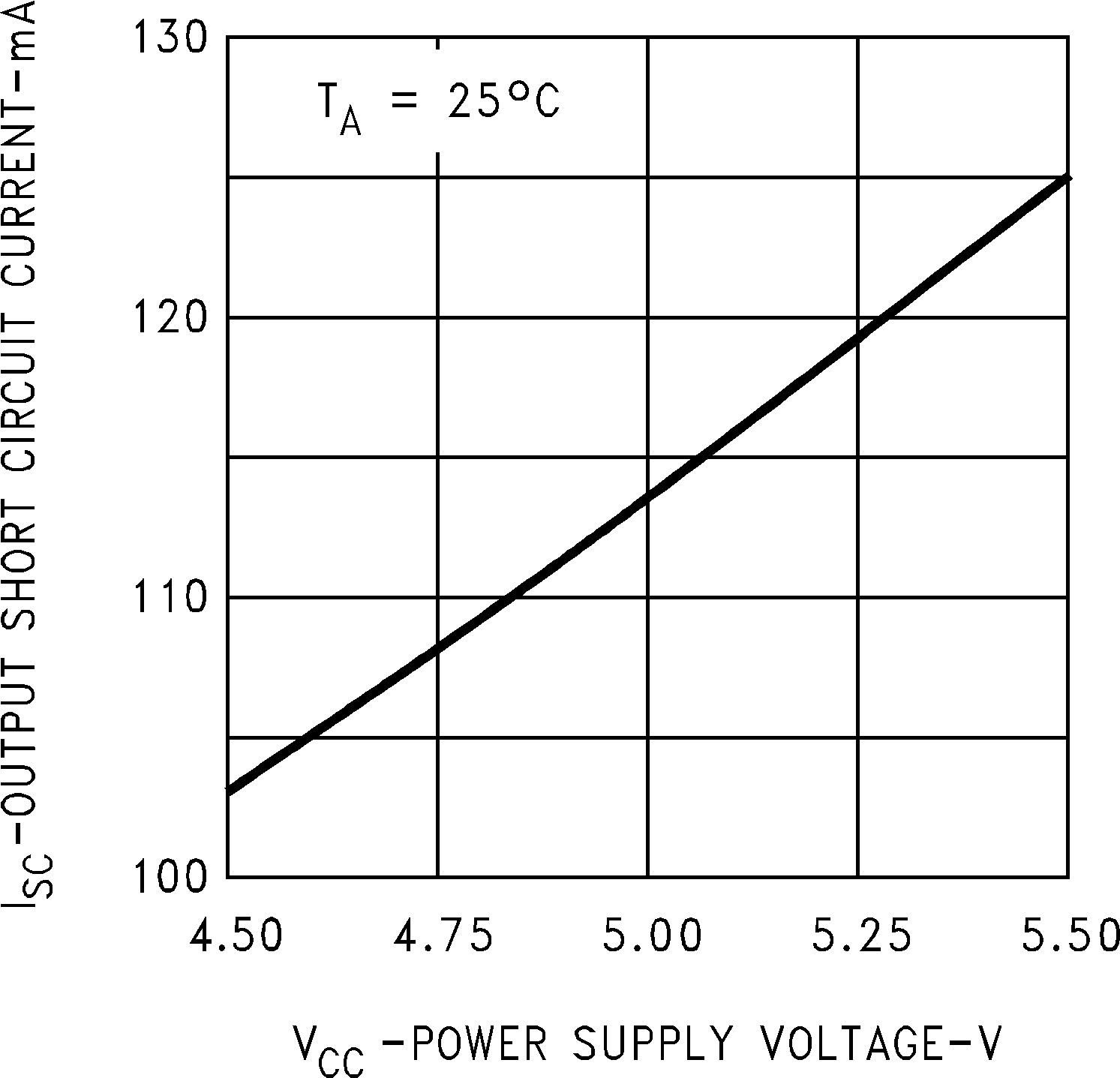
 Figure 2. Differential Propagation Delay vs Power Supply Voltage
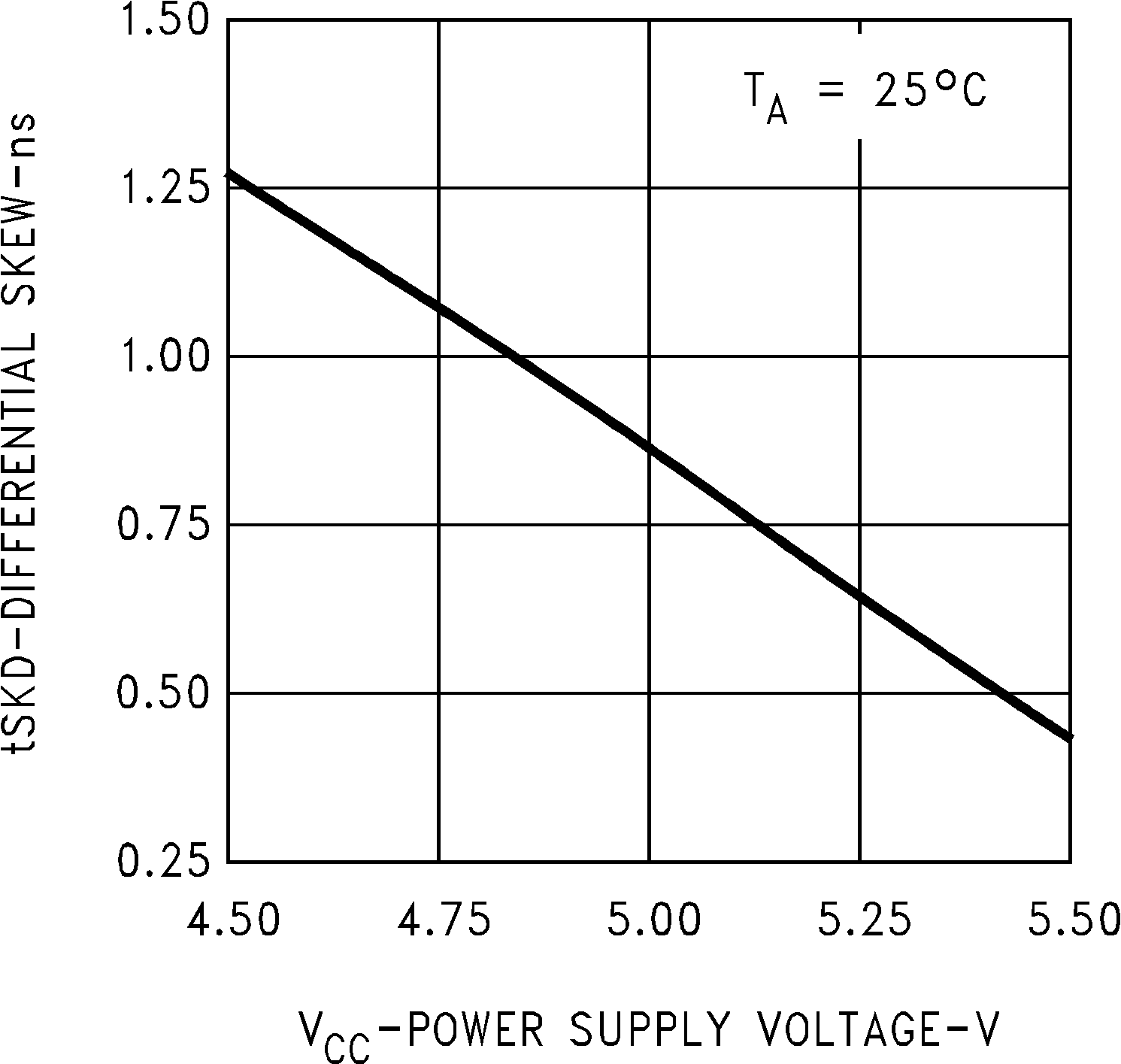 Figure 4. Differential Skew vs Power Supply Voltage
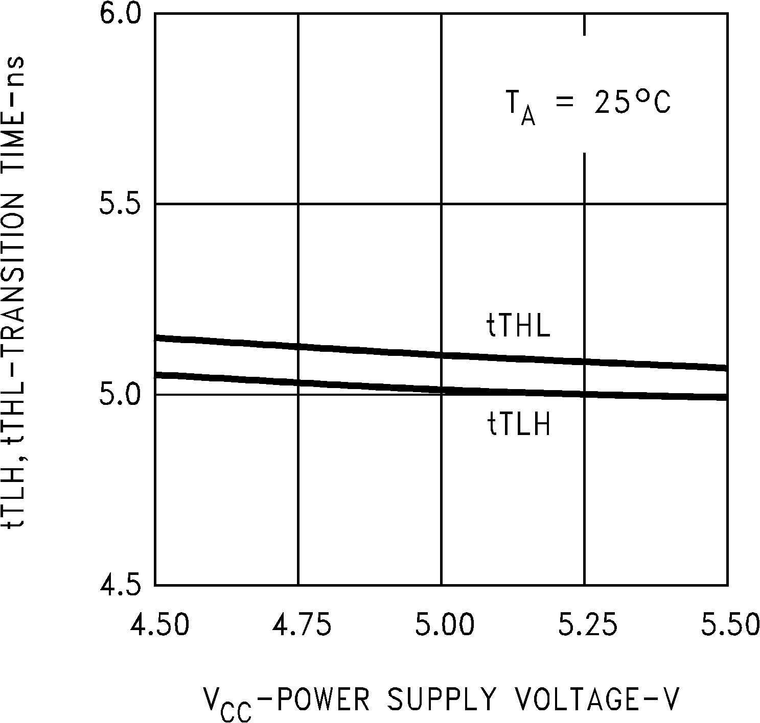 Figure 6. Differential Transition Time vs Power Supply Voltage
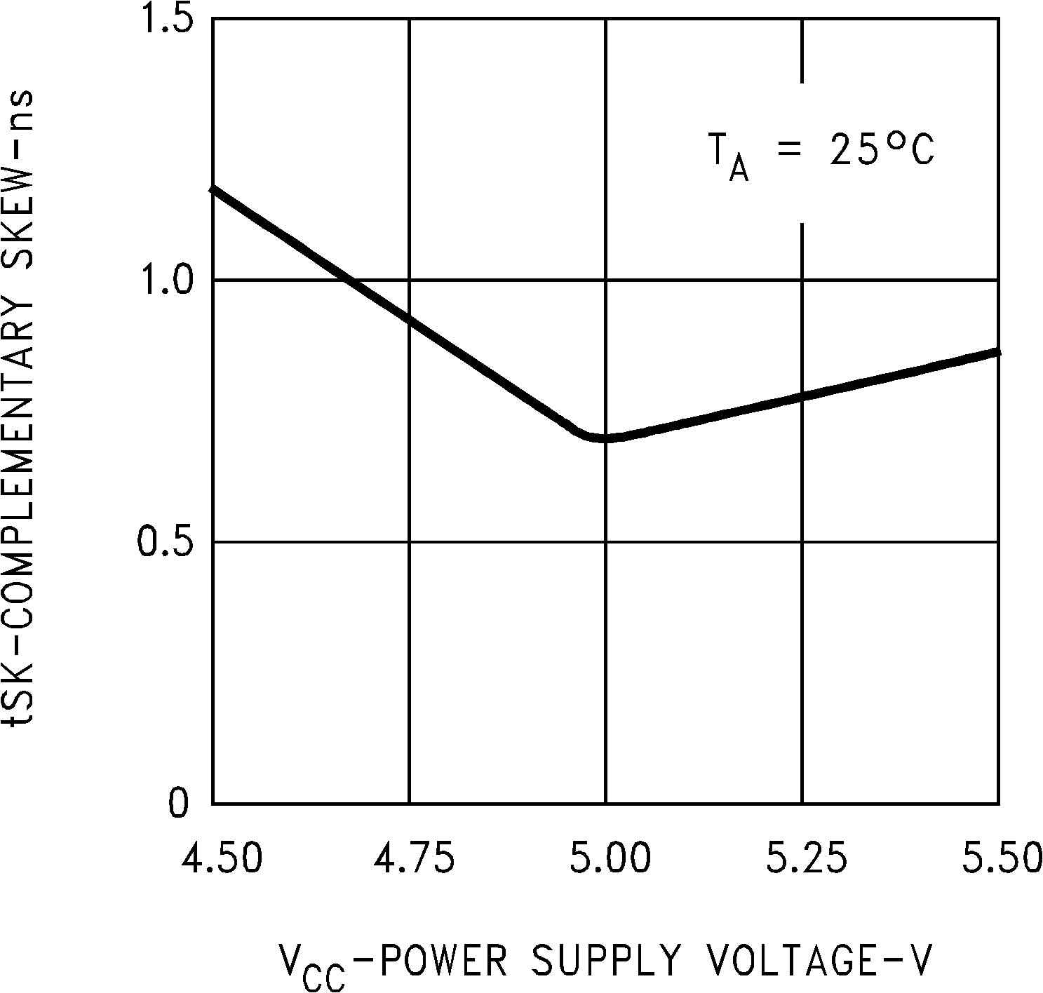 Figure 8. Complementary Skew vs Power Supply Voltage
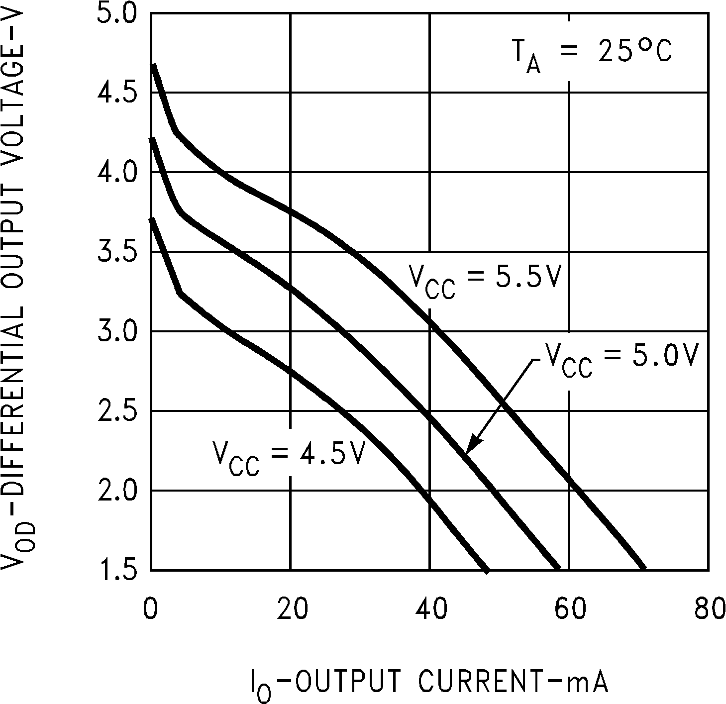 Figure 10. Differential Output Voltage vs Output Current
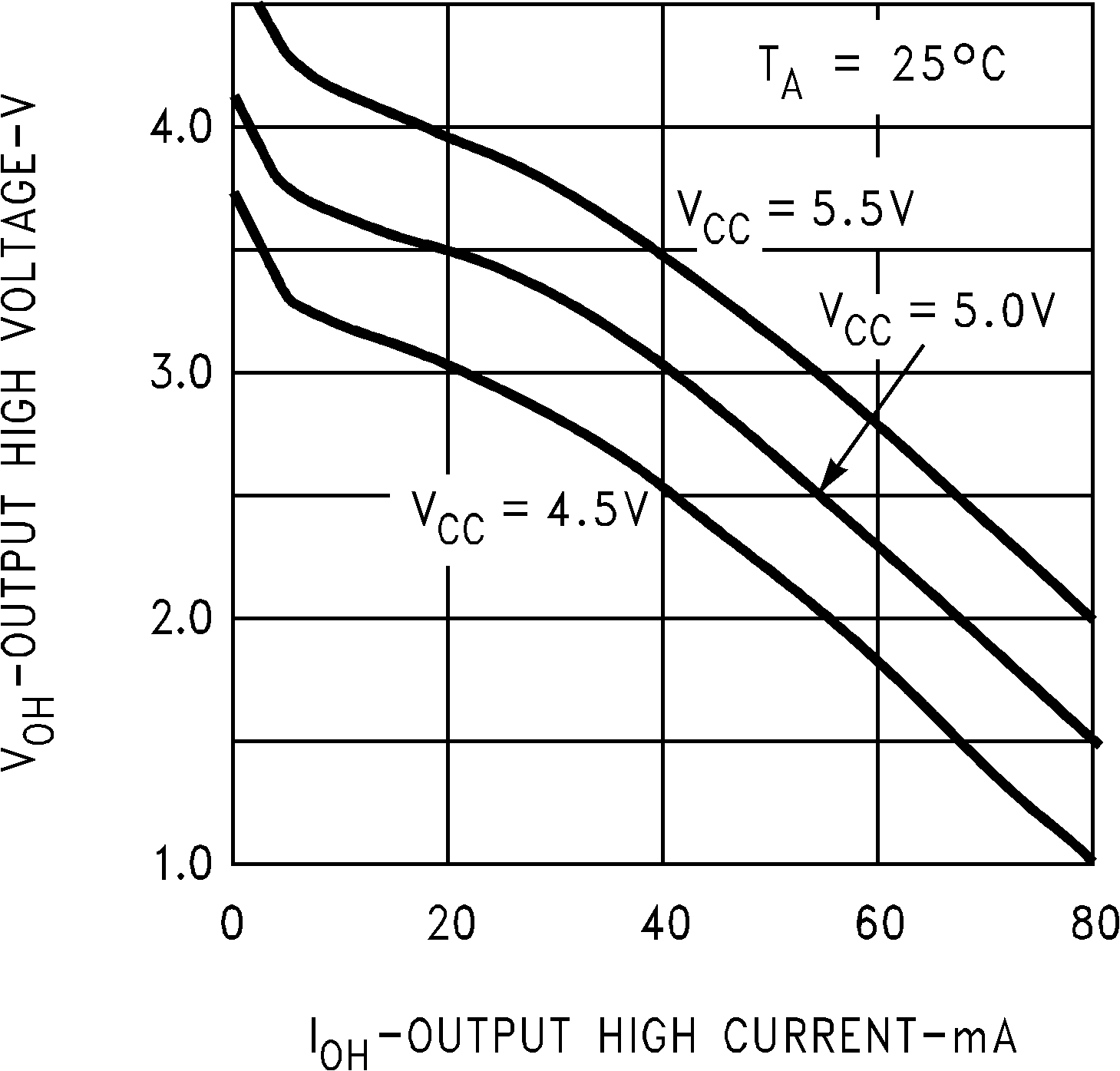 Figure 12. Output High Voltage vs Output High Current
Figure 14. Output Low Voltage vs Output Low Current
Figure 16. Output Low Voltage vs Output Low Current
Figure 18. Supply Current vs Temperature
Figure 12. Output High Voltage vs Output High Current
Figure 14. Output Low Voltage vs Output Low Current
Figure 16. Output Low Voltage vs Output Low Current
Figure 18. Supply Current vs Temperature
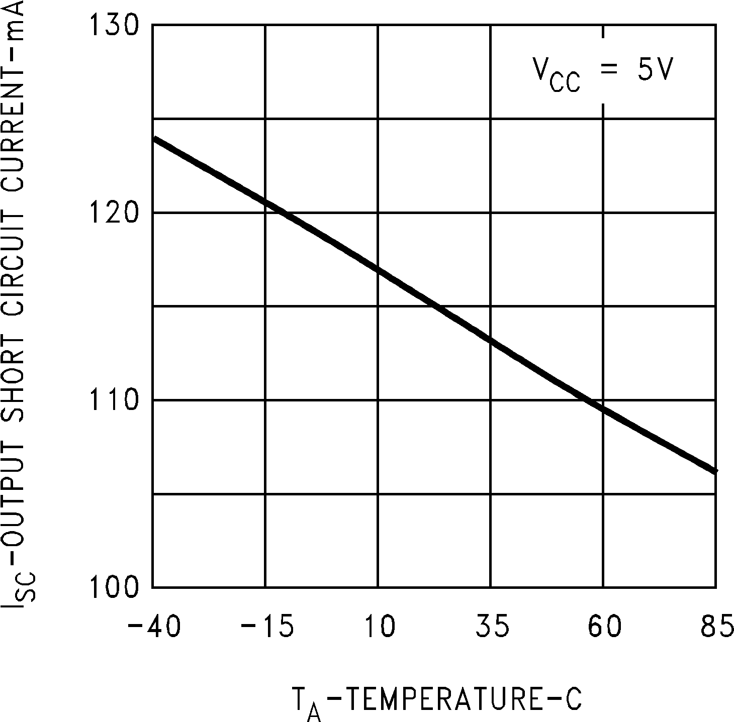 Figure 20. Output Short Circuit Current vs Temperature