ZHCSCU6A June 2014 – September 2014 ULN2003B
PRODUCTION DATA.
- 1 特性
- 2 应用
- 3 说明
- 4 简化电路原理图
- 5 修订历史记录
- 6 Pin Configuration and Functions
-
7 Specifications
- 7.1 Absolute Maximum Ratings
- 7.2 Handling Ratings
- 7.3 Recommended Operating Conditions
- 7.4 Thermal Information
- 7.5 Electrical Characteristics, TA = 25°C
- 7.6 Electrical Characteristics, TA = -40°C to 105°C
- 7.7 Switching Characteristics, TA = 25°C
- 7.8 Switching Characteristics, TA = -40°C to 105°C
- 7.9 Typical Characteristics
- 7.10 Thermal Information
- 8 Parameter Measurement Information
- 9 Detailed Description
- 10Application and Implementation
- 11Power Supply Recommendations
- 12Layout
- 13器件和文档支持
- 14机械封装和可订购信息
9 Detailed Description
9.1 Overview
This standard device has proven ubiquity and versatility across a wide range of applications. This is due to it's integration of 7 Darlington transistors that are capable of sinking up to 500 mA and wide GPIO range capability.
The ULN2003B comprises seven high voltage, high current NPN Darlington transistor pairs. All units feature a common emitter and open collector outputs. To maximize their effectiveness, these units contain suppression diodes for inductive loads. The ULN2003B has a series base resistor to each Darlington pair, thus allowing operation directly with TTL or CMOS operating at supply voltages of 5.0 V or 3.3 V. The ULN2003B offers solutions to a great many interface needs, including solenoids, relays, lamps, small motors, and LEDs. Applications requiring sink currents beyond the capability of a single output may be accommodated by paralleling the outputs.
This device can operate over a wide temperature range (–40°C to 105°C).
9.2 Functional Block Diagram
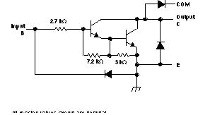 Figure 15. Schematic (Each Comparator)
9.3 Feature Description
Each channel of ULN2003B consists of Darlington connected NPN transistors. This connection creates the effect of a single transistor with a very high current gain (β2). This can be as high as 10,000 A/A at certain currents. The very high β allows for high output current drive with a very low input current, essentially equating to operation with low GPIO voltages.
The GPIO voltage is converted to base current via the 2.7 kΩ resistor connected between the input and base of the pre-driver Darlington NPN. The 7.2 kΩ & 3.0 kΩ resistors connected between the base and emitter of each respective NPN act as pull-downs and suppress the amount of leakage that may occur from the input.
The diodes connected between the output and COM pin is used to suppress the kick-back voltage from an inductive load that is excited when the NPN drivers are turned off (stop sinking) and the stored energy in the coils causes a reverse current to flow into the coil supply via the kick-back diode.
In normal operation the diodes on base and collector pins to emitter will be reversed biased. If these diode are forward biased, internal parasitic NPN transistors will draw (a nearly equal) current from other (nearby) device pins.
9.4 Device Functional Modes
9.4.1 Inductive Load Drive
When the COM pin is tied to the coil supply voltage, ULN2003B is able to drive inductive loads and supress the kick-back voltage via the internal free wheeling diodes.
9.4.2 Resistive Load Drive
When driving a resistive load, a pull-up resistor is needed in order for ULN2003B to sink current and for there to be a logic high level. The COM pin can be left floating for these applications.