ZHCSCU6A June 2014 – September 2014 ULN2003B
PRODUCTION DATA.
- 1 特性
- 2 应用
- 3 说明
- 4 简化电路原理图
- 5 修订历史记录
- 6 Pin Configuration and Functions
-
7 Specifications
- 7.1 Absolute Maximum Ratings
- 7.2 Handling Ratings
- 7.3 Recommended Operating Conditions
- 7.4 Thermal Information
- 7.5 Electrical Characteristics, TA = 25°C
- 7.6 Electrical Characteristics, TA = -40°C to 105°C
- 7.7 Switching Characteristics, TA = 25°C
- 7.8 Switching Characteristics, TA = -40°C to 105°C
- 7.9 Typical Characteristics
- 7.10 Thermal Information
- 8 Parameter Measurement Information
- 9 Detailed Description
- 10Application and Implementation
- 11Power Supply Recommendations
- 12Layout
- 13器件和文档支持
- 14机械封装和可订购信息
7 Specifications
7.1 Absolute Maximum Ratings(1)
at 25°C free-air temperature (unless otherwise noted)| MIN | MAX | UNIT | |||
|---|---|---|---|---|---|
| VCC | Collector-emitter voltage | 50 | V | ||
| Clamp diode reverse voltage(2) | 50 | V | |||
| VI | Input voltage(2) | 30 | V | ||
| Peak collector current(3)(4) | 500 | mA | |||
| IOK | Output clamp current | 500 | mA | ||
| Total emitter-terminal current | –2.5 | A | |||
| TA | Operating free-air temperature range | –40 | 105 | °C | |
| θJA | Package thermal impedance(3)(4) | D package | 81 | °C/W | |
| N package | 49.7 | ||||
| PW package | 105 | ||||
| TJ | Operating virtual junction temperature | 150 | °C | ||
(1) Stresses beyond those listed under "absolute maximum ratings" may cause permanent damage to the device. These are stress ratings only, and functional operation of the device at these or any other conditions beyond those indicated under "recommended operating conditions" is not implied. Exposure to absolute-maximum-rated conditions for extended periods may affect device reliability.
(2) All voltage values are with respect to the emitter/substrate terminal E, unless otherwise noted.
(3) Maximum power dissipation is a function of TJ(max), θJA, and TA. The maximum allowable power dissipation at any allowable ambient temperature is PD = (TJ(max) – TA)/θJA. Operating at the absolute maximum TJ of 150°C can affect reliability.
(4) The package thermal impedance is calculated in accordance with JESD 51-7.
7.2 Handling Ratings
| MIN | MAX | UNIT | |||
|---|---|---|---|---|---|
| Tstg | Storage temperature range | –65 | 150 | °C | |
| V(ESD) | Electrostatic discharge | Human body model (HBM), per ANSI/ESDA/JEDEC JS-001, all pins(1) | 2000 | V | |
| Charged device model (CDM), per JEDEC specification JESD22-C101, all pins(2) | 500 | ||||
(1) JEDEC document JEP155 states that 500-V HBM allows safe manufacturing with a standard ESD control process.
(2) JEDEC document JEP157 states that 250-V CDM allows safe manufacturing with a standard ESD control process.
7.3 Recommended Operating Conditions
over operating free-air temperature range (unless otherwise noted)| MIN | MAX | UNIT | ||
|---|---|---|---|---|
| VI | 0 | 5 | V | |
| VCC | 0 | 50 | V | |
| TJ | Junction Temperature | -40 | 125 | °C |
7.4 Thermal Information
| THERMAL METRIC(1) | ULN2003B | UNIT | ||
|---|---|---|---|---|
| PW | D | |||
| 16 PINS | 16 PINS | |||
| RθJA | Junction-to-ambient thermal resistance | 105.4 | 81.2 | °C/W |
| RθJCtop | Junction-to-case (top) thermal resistance | 32.9 | 40.3 | |
| RθJB | Junction-to-board thermal resistance | 51.3 | 38.9 | |
| ψJT | Junction-to-top characterization parameter | 2.1 | 10.9 | |
| ψJB | Junction-to-board characterization parameter | 50.6 | 38.7 | |
(1) For more information about traditional and new thermal metrics, see the IC Package Thermal Metrics application report, SPRA953.
7.5 Electrical Characteristics, TA = 25°C
| PARAMETER | TEST FIGURE | TEST CONDITIONS | ULN2003B | UNIT | ||||
|---|---|---|---|---|---|---|---|---|
| MIN | TYP | MAX | ||||||
| VI(on) | On-state input voltage | Figure 12 | VCE = 2 V | IC = 200 mA | 2.4 | V | ||
| IC = 250 mA | 2.7 | |||||||
| IC = 300 mA | 3 | |||||||
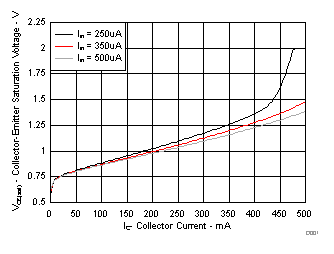
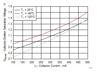
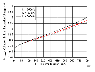
| VCE(sat) | Collector-emitter saturation voltage | Figure 11 | II = 250 μA, | IC = 100 mA | 0.9 | 1.1 | V | |
| II = 350 μA, | IC = 200 mA | 1 | 1.3 | |||||
| II = 500 μA, | IC = 350 mA | 1.2 | 1.6 | |||||
| ICEX | Collector cutoff current | Figure 8 | VCE = 50 V, | II = 0 | 10 | μA | ||
| VF | Clamp forward voltage | Figure 14 | IF = 350 mA | 1.7 | 2 | V | ||
| II(off) | Off-state input current | Figure 9 | VCE = 50 V, | IC = 500 μA | 50 | 65 | μA | |
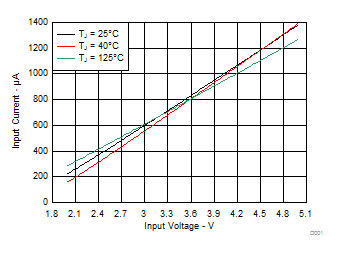
| II | Input current | Figure 10 | VI = 3.85 V | 0.93 | 1.35 | mA | ||
| IR | Clamp reverse current | Figure 13 | VR = 50 V | 50 | μA | |||
| Ci | Input capacitance | VI = 0, | f = 1 MHz | 15 | 25 | pF | ||
7.6 Electrical Characteristics, TA = –40°C to 105°C
| PARAMETER | TEST FIGURE | TEST CONDITIONS | ULN2003B | UNIT | ||||
|---|---|---|---|---|---|---|---|---|
| MIN | TYP | MAX | ||||||
| VI(on) | On-state input voltage | Figure 12 | VCE = 2 V | IC = 200 mA | 2.7 | V | ||
| IC = 250 mA | 2.9 | |||||||
| IC = 300 mA | 3 | |||||||
| VCE(sat) | Collector-emitter saturation voltage | Figure 11 | II = 250 μA, | IC = 100 mA | 0.9 | 1.2 | V | |
| II = 350 μA, | IC = 200 mA | 1 | 1.4 | |||||
| II = 500 μA, | IC = 350 mA | 1.2 | 1.7 | |||||
| ICEX | Collector cutoff current | Figure 8 | VCE = 50 V, | II = 0 | 20 | μA | ||
| VF | Clamp forward voltage | Figure 14 | IF = 350 mA | 1.7 | 2.2 | V | ||
| II(off) | Off-state input current | Figure 9 | VCE = 50 V, | IC = 500 μA | 30 | 65 | μA | |
| II | Input current | Figure 10 | VI = 3.85 V | 0.93 | 1.35 | mA | ||
| IR | Clamp reverse current | Figure 13 | VR = 50 V | 100 | μA | |||
| Ci | Input capacitance | VI = 0, | f = 1 MHz | 15 | 25 | pF | ||
7.7 Switching Characteristics, TA = 25°C
| PARAMETER | TEST CONDITIONS | MIN | TYP | MAX | UNIT | ||
|---|---|---|---|---|---|---|---|
| tPLH | Propagation delay time, low- to high-level output | 0.25 | 1 | μs | |||
| tPHL | Propagation delay time, high- to low-level output | 0.25 | 1 | μs | |||
| VOH | High-level output voltage after switching | VS = 50 V, | IO ≈ 300 mA | VS – 20 | mV | ||
7.8 Switching Characteristics, TA = –40°C to 105°C
| PARAMETER | TEST CONDITIONS | MIN | TYP | MAX | UNIT | ||
|---|---|---|---|---|---|---|---|
| tPLH | Propagation delay time, low- to high-level output | 1 | 10 | μs | |||
| tPHL | Propagation delay time, high- to low-level output | 1 | 10 | μs | |||
| VOH | High-level output voltage after switching | VS = 50 V, | IO ≈ 300 mA | VS – 50 | mV | ||
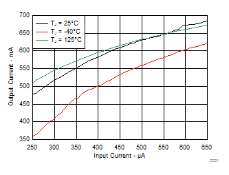
7.9 Typical Characteristics
7.10 Thermal Information
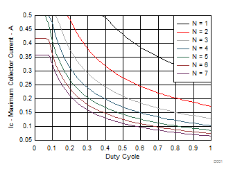 Figure 6. D Package Maximum collector Current vs Duty Cycle
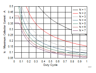 Figure 7. PW Package Maximum collector Current vs Duty Cycle