ZHCSCU6A June 2014 – September 2014 ULN2003B
PRODUCTION DATA.
- 1 特性
- 2 应用
- 3 说明
- 4 简化电路原理图
- 5 修订历史记录
- 6 Pin Configuration and Functions
-
7 Specifications
- 7.1 Absolute Maximum Ratings
- 7.2 Handling Ratings
- 7.3 Recommended Operating Conditions
- 7.4 Thermal Information
- 7.5 Electrical Characteristics, TA = 25°C
- 7.6 Electrical Characteristics, TA = -40°C to 105°C
- 7.7 Switching Characteristics, TA = 25°C
- 7.8 Switching Characteristics, TA = -40°C to 105°C
- 7.9 Typical Characteristics
- 7.10 Thermal Information
- 8 Parameter Measurement Information
- 9 Detailed Description
- 10Application and Implementation
- 11Power Supply Recommendations
- 12Layout
- 13器件和文档支持
- 14机械封装和可订购信息
10 Application and Implementation
NOTE
Information in the following applications sections is not part of the TI component specification, and TI does not warrant its accuracy or completeness. TI’s customers are responsible for determining suitability of components for their purposes. Customers should validate and test their design implementation to confirm system functionality.
10.1 Application Information
ULN2003B will typically be used to drive a high voltage and/or current peripheral from an MCU or logic device that cannot tolerate these conditions. The following design is a common application of ULN2003B, driving inductive loads. This includes motors, solenoids & relays. Each load type can be modeled by what's seen in Figure 16.
10.2 Typical Application
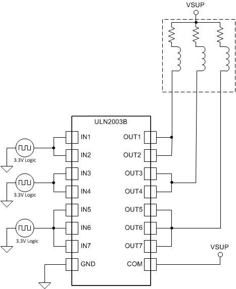 Figure 16. ULN2003B as Inductive Load Driver
10.2.1 Design Requirements
For this design example, use the parameters listed in Table 1 as the input parameters.
Table 1. Design Parameters
| DESIGN PARAMETER | EXAMPLE VALUE |
|---|---|
| GPIO Voltage | 3.3 V or 5.0 V |
| Coil Supply Voltage | 12 V to 48 V |
| Number of Channels | 7 |
| Output Current (RCOIL) | 20 mA to 300 mA per channel |
| Duty Cycle | 100% |
10.2.2 Detailed Design Procedure
When using ULN2003B in a coil driving application, determine the following:
- Input Voltage Range
- Temperature Range
- Output & Drive Current
- Power Dissipation
10.2.2.1 Drive Current
The coil current is determined by the coil voltage (VSUP), coil resistance & output low voltage (VOL or VCE(SAT)).
10.2.2.2 Output Low Voltage
The output low voltage (VOL) is the same thing as VCE(SAT) and can be determined by, Figure 1, Figure 2, or Figure 5.
10.2.2.3 Power Dissipation & Temperature
The number of coils driven is dependent on the coil current and on-chip power dissipation. The number of coils driven can be determined by Figure 6 or Figure 7.
For a more accurate determination of number of coils possible, use the below equation to calculate ULN2003B on-chip power dissipation PD:
In order to guarantee reliability of ULN2003B and the system the on-chip power dissipation must be lower that or equal to the maximum allowable power dissipation (PD(MAX)) dictated by below equation Equation 3.
It is recommended to limit ULN2003B IC’s die junction temperature to less than 125°C. The IC junction temperature is directly proportional to the on-chip power dissipation.
10.2.3 Application Curves
The following curves were generated with ULN2003B driving an OMRON G5NB relay – Vin = 5.0V; Vsup= 12 V & RCOIL= 2.8 kΩ
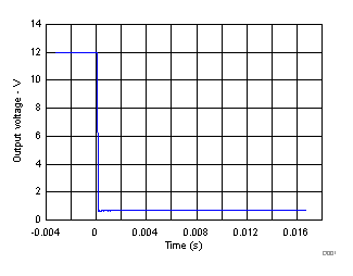 Figure 17. Output Response With Activation of Coil (Turn On)
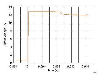 Figure 18. Output Response With De-activation of Coil (Turn Off)