ZHCSK45C august 2019 – december 2020 UCC28740-Q1
PRODUCTION DATA
- 1
- 1 特性
- 2 应用
- 3 说明
- 4 Revision History
- 5 Revision History
- 6 Revision History
- 7 Pin Configuration and Functions
- 8 Specifications
- 9 Detailed Description
-
10Application and Implementation
- 10.1 Application Information
- 10.2 High Voltage Applications
- 10.3
Typical Application
- 10.3.1 Design Requirements
- 10.3.2
Detailed Design Procedure
- 10.3.2.1 Custom Design With WEBENCH® Tools
- 10.3.2.2 Standby Power Estimate and No-Load Switching Frequency
- 10.3.2.3 Input Bulk Capacitance and Minimum Bulk Voltage
- 10.3.2.4 38
- 10.3.2.5 Transformer Turns-Ratio, Inductance, Primary Peak Current
- 10.3.2.6 Transformer Parameter Verification
- 10.3.2.7 VS Resistor Divider, Line Compensation
- 10.3.2.8 Output Capacitance
- 10.3.2.9 VDD Capacitance, CVDD
- 10.3.2.10 Feedback Network Biasing
- 10.3.3 Application Curves
- 11Power Supply Recommendations
- 12Layout
-
13Device and Documentation Support
- 13.1
Device Support
- 13.1.1 Development Support
- 13.1.2
Device Nomenclature
- 13.1.2.1 Capacitance Terms in Farads
- 13.1.2.2 Duty Cycle Terms
- 13.1.2.3 Frequency Terms in Hertz
- 13.1.2.4 Current Terms in Amperes
- 13.1.2.5 Current and Voltage Scaling Terms
- 13.1.2.6 Transformer Terms
- 13.1.2.7 Power Terms in Watts
- 13.1.2.8 Resistance Terms in Ohms
- 13.1.2.9 Timing Terms in Seconds
- 13.1.2.10 Voltage Terms in Volts
- 13.1.2.11 AC Voltage Terms in VRMS
- 13.1.2.12 Efficiency Terms
- 13.2 Documentation Support
- 13.3 Receiving Notification of Documentation Updates
- 13.4 Community Resources
- 13.5 Trademarks
- 13.1
Device Support
- Mechanical, Packaging, and Orderable Information
9.4.2 Primary-Side Constant-Current (CC) Regulation
When the load current of the converter increases to the predetermined constant-current limit, operation enters CC mode. In CC mode, output voltage regulation is lost and the shunt-regulator drives the current and voltage at FB to minimum. During CC mode, timing information at the VS pin and current information at the CS pin allow accurate regulation of the average current of the secondary winding. The CV-regulation control law dictates that as load increases approaches CC regulation the primary peak current will be at IPP(max). The primary peak current, turns-ratio, demagnetization time tDM, and switching period tSW determine the secondary average output current (see Figure 9-6). Ignoring leakage-inductance effects, the average output current is given by Equation 5. When the demagnetization duty-cycle reaches the CC-regulation reference, DMAGCC, in the current-control block, the controller operates in frequency modulation (FM) mode to control the output current for any output voltage at or below the voltage-regulation target as long as the auxiliary winding keeps VVDD above the UVLO turnoff threshold. As the output voltage falls, tDM increases. The controller acts to increase tSW to maintain the ratio of tDM to switching period (tDM / tSW) at a maximum of 0.425 (DMAGCC), thereby maintaining a constant average output current.
 Figure 9-6 Transformer-Current Relationship
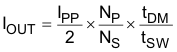
Fast, accurate, opto-coupled CV control combined with line-compensated PSR CC control results in high-performance voltage and current regulation which minimizes voltage deviations due to heavy load and unload steps, as illustrated by the V-I curve in Figure 9-7.
 Figure 9-7 Typical Target Output V-I Characteristic