ZHCSN70F November   2002  – November 2023 UCC27423 , UCC27424 , UCC27425

PRODUCTION DATA  

  1.   1
  2. 特性
  3. 应用
  4. 说明
  5. Device Comparison Table
  6. Pin Configuration and Functions
  7. Specifications
    1. 6.1 Absolute Maximum Ratings
    2. 6.2 ESD Ratings
    3. 6.3 Recommended Operating Conditions
    4. 6.4 Thermal Information
    5. 6.5 Electrical Characteristics
    6. 6.6 Dissipation Ratings
    7. 6.7 Typical Characteristics
  8. Detailed Description
    1. 7.1 Overview
    2. 7.2 Functional Block Diagram
    3. 7.3 Feature Description
      1. 7.3.1 Enable
      2. 7.3.2 Input Stage
      3. 7.3.3 Output Stage
    4. 7.4 Device Functional Modes
  9. Application and Implementation
    1. 8.1 Application Information
    2. 8.2 Typical Application
      1. 8.2.1 Design Requirements
      2. 8.2.2 Detailed Design Procedure
        1. 8.2.2.1 Source and Sink Capabilities During Miller Plateau
        2. 8.2.2.2 Parallel Outputs
        3. 8.2.2.3 VDD
        4. 8.2.2.4 Drive Current and Power Requirements
      3. 8.2.3 Application Curves
  10. Power Supply Recommendations
  11. 10Layout
    1. 10.1 Layout Guidelines
    2. 10.2 Layout Example
    3. 10.3 Thermal Considerations
  12. 11Device and Documentation Support
    1. 11.1 Device Support
      1. 11.1.1 第三方产品免责声明
    2. 11.2 Documentation Support
      1. 11.2.1 Related Documentation
    3. 11.3 接收文档更新通知
    4. 11.4 支持资源
    5. 11.5 Trademarks
    6. 11.6 静电放电警告
    7. 11.7 术语表
  13. 12Revision History
  14. 13Mechanical, Packaging, and Orderable Information

封装选项

请参考 PDF 数据表获取器件具体的封装图。

机械数据 (封装 | 引脚)
  • D|8
  • P|8
  • DGN|8
散热焊盘机械数据 (封装 | 引脚)
订购信息

Application Curves

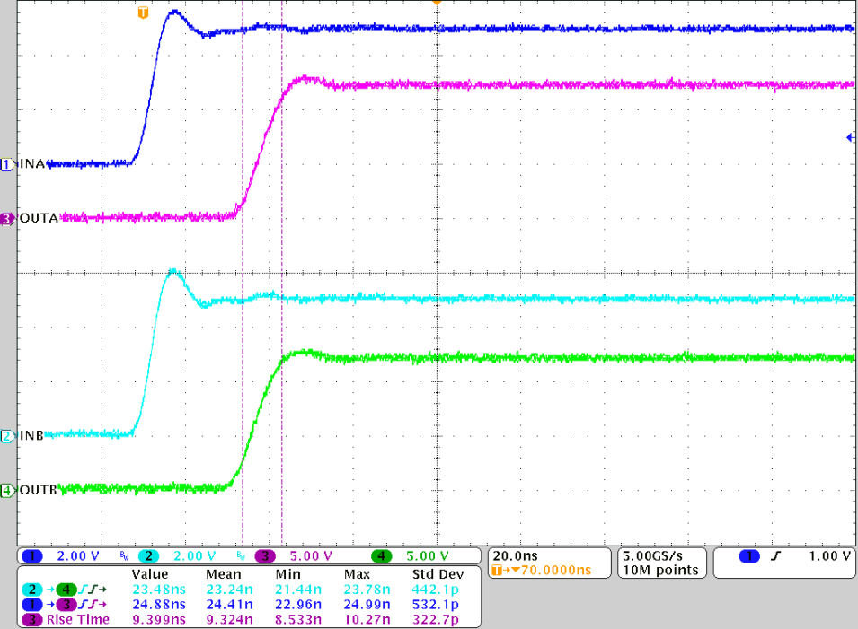
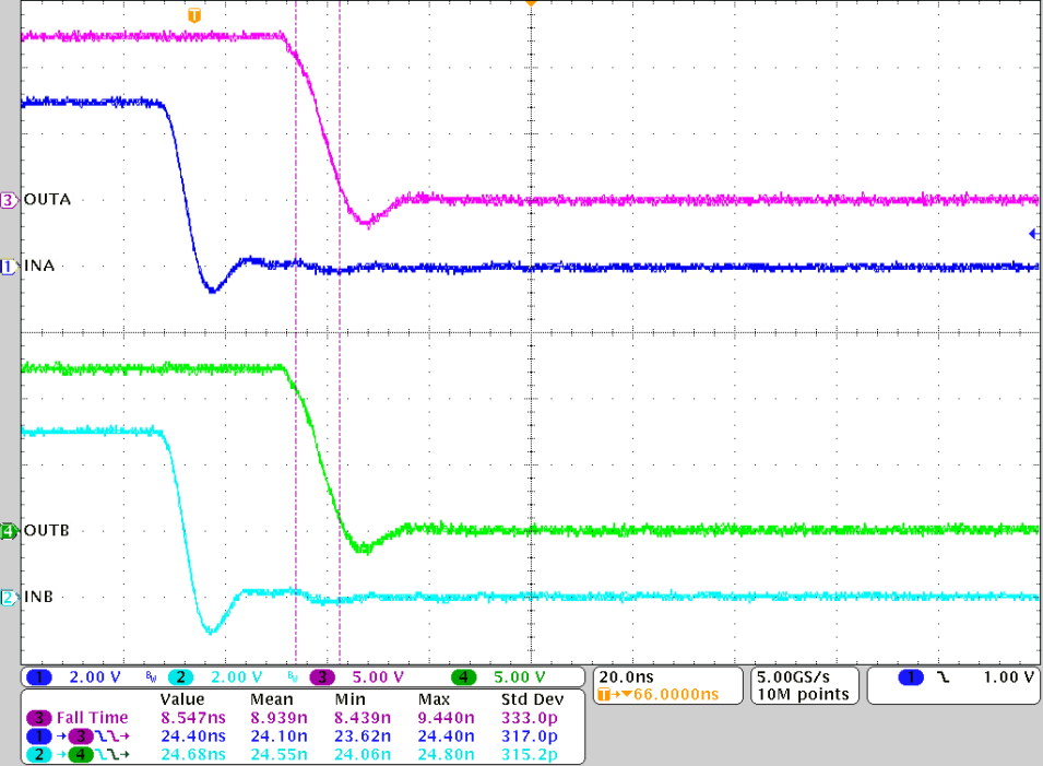
Figure 8-5 and Figure 8-6 shows rising/falling time and turn-on/off propagation delay testing waveform in room temperature for UCC27424, and waveform measurement data (see the bottom part of the waveform). Each channel, INA/INB/OUTA/OUTB, is labeled and displayed on the left hand of the waveforms.

The load capacitance testing condition is 1.8 nF, VDD = 12 V, and f = 300 kHz.

HI and LI share one same input from function generator, therefore, besides the propagation delay and rising/falling time, the difference of the propagation delay between HO and LO gives the propagation delay matching data.

Note the linear rise and fall edges of the switching waveforms. This is due to the constant output current characteristic of the driver as opposed to the resistive output impedance of traditional MOSFET-based gate drivers.
GUID-1A586F69-C1D6-43DA-B6A7-7D99B0AEE705-low.png
CL = 1.8 nF, VDD = 12 V, f = 300 kHz
Figure 8-5 Rising Time and Turnon Propagation Delay
GUID-3D393E9D-F10E-4BD4-96F5-B417A7C9ABC2-low.png
CL = 1.8 nF, VDD = 12 V, f = 300 kHz
Figure 8-6 Falling Time and Turnoff Propagation Delay