ZHCSN70F November 2002 – November 2023 UCC27423 , UCC27424 , UCC27425
PRODUCTION DATA
- 1
- 1 特性
- 2 应用
- 3 说明
- 4 Device Comparison Table
- 5 Pin Configuration and Functions
- 6 Specifications
- 7 Detailed Description
- 8 Application and Implementation
- 9 Power Supply Recommendations
- 10Layout
- 11Device and Documentation Support
- 12Revision History
- 13Mechanical, Packaging, and Orderable Information
封装选项
请参考 PDF 数据表获取器件具体的封装图。
机械数据 (封装 | 引脚)
- D|8
- P|8
- DGN|8
散热焊盘机械数据 (封装 | 引脚)
- DGN|8
订购信息
8.2.2.4 Drive Current and Power Requirements
The UCC2742x family of drivers are capable of delivering 4 A of current to a MOSFET gate for a period of several hundred nanoseconds. High peak current is required to turn the device ON quickly. Then, to turn the device OFF, the driver is required to sink a similar amount of current to ground. This repeats at the operating frequency of the power device. A MOSFET is used in this discussion because it is the most common type of switching device used in high frequency power conversion equipment.
References 1 and 2 in Section 11.2 discuss the current required to drive a power MOSFET and other capacitive-input switching devices. Reference 2 in Section 11.2 includes information on the previous generation of bipolar IC gate drivers.
When a driver IC is tested with a discrete, capacitive load it is a fairly simple matter to calculate the power that is required from the bias supply. The energy that must be transferred from the bias supply to charge the capacitor is given by Equation 2.

where
- C = load capacitor, and V = bias voltage (feeding the driver)
There is an equal amount of energy transferred to ground when the capacitor is discharged. This leads to a power loss given by Equation 3.
where
- f = switching frequency
This power is dissipated in the resistive elements of the circuit. Thus, with no external resistor between the driver and gate, this power is dissipated inside the driver. Half of the total power is dissipated when the capacitor is charged, and the other half is dissipated when the capacitor is discharged. An actual example using the conditions of the previous gate drive waveform should help clarify this.
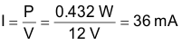
With VDD = 12 V, CLOAD = 10 nF, and f = 300 kHz, the power loss can be calculated as Equation 4.
With a 12 V supply, this would equate to a current of Equation 5.
The actual current measured from the supply was 0.037A, and is very close to the predicted value. But, the IDD current that is due to the IC internal consumption should be considered. With no load the IC current draw is 0.0027 A. Under this condition the output rise and fall times are faster than with a load. This could lead to an almost insignificant, yet measurable current due to cross-conduction in the output stages of the driver. However, these small current differences are buried in the high frequency switching spikes, and are beyond the measurement capabilities of a basic lab setup. The measured current with 10 nF load is reasonably close to that expected.
The switching load presented by a power MOSFET can be converted to an equivalent capacitance by examining the gate charge required to switch the device. This gate charge includes the effects of the input capacitance plus the added charge needed to swing the drain of the device between the ON and OFF states. Most manufacturers provide specifications that provide the typical and maximum gate charge, in nC, to switch the device under specified conditions. Using the gate charge Qg, one can determine the power that must be dissipated when charging a capacitor. This is done by using the equivalence Qg = CeffV to provide the power loss in Equation 6.
This equation allows a power designer to calculate the bias power required to drive a specific MOSFET gate at a specific bias voltage.