ZHCSIL2C July 2018 – March 2022 UCC24624
PRODUCTION DATA
- 1 特性
- 2 应用
- 3 说明
- 4 Revision History
- 5 说明(续)
- 6 Pin Configuration and Functions
- 7 Specifications
- 8 Detailed Description
- 9 Application and Implementation
- 10Power Supply Recommendations
- 11Layout
- 12Device and Documentation Support
9.2.3 Application Curves
The typical operation waveforms, as well as the efficiency performance are summarized in following sections.
- CH1 = VG1(TP4), CH3 = Q1 drain (TP2), CH2 = VG2(TP5), CH4 = Q1 drain (TP3)
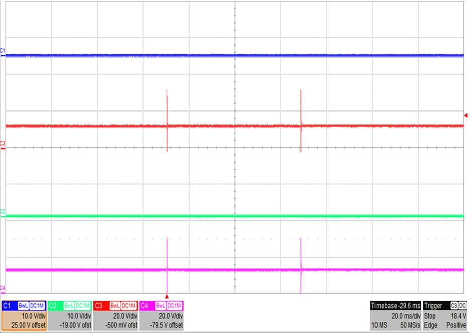 Figure 9-2 VIN = 340 V, IOUT = 0 A, No Gate Drive Under Light Load (VG1, VG2)
 Figure 9-4 VIN = 340 V, IOUT = 10 A Full Load
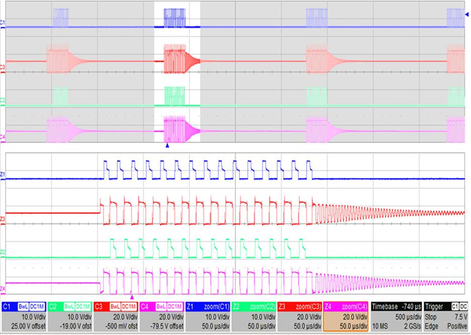 Figure 9-3 VIN = 340 V, IOUT = 0.3 A, LLC is Operating In Burst Mode
 Figure 9-5 VIN = 390 V, IOUT = 0 A, No Gate Drive Under Light Load (VG1, VG2)
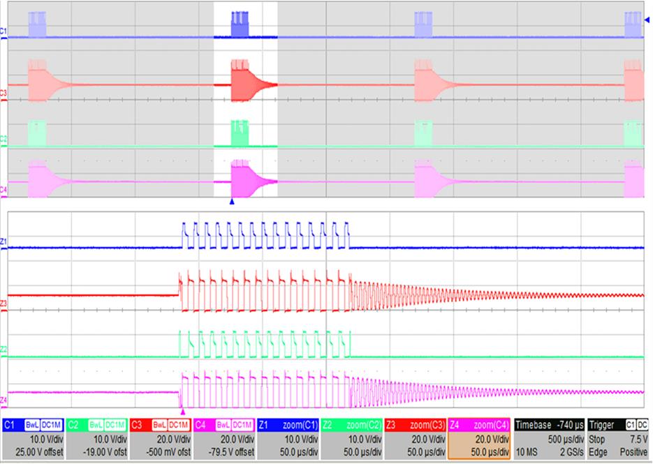 Figure 9-6 VIN = 390 V, IOUT = 0.3 A, LLC is Operating In Burst Mode
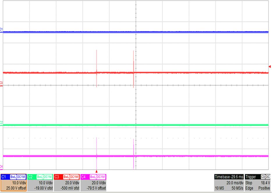 Figure 9-8 VIN = 410 V, IOUT = 0 A, No Gate Drive Under Light Load (VG1, VG2)
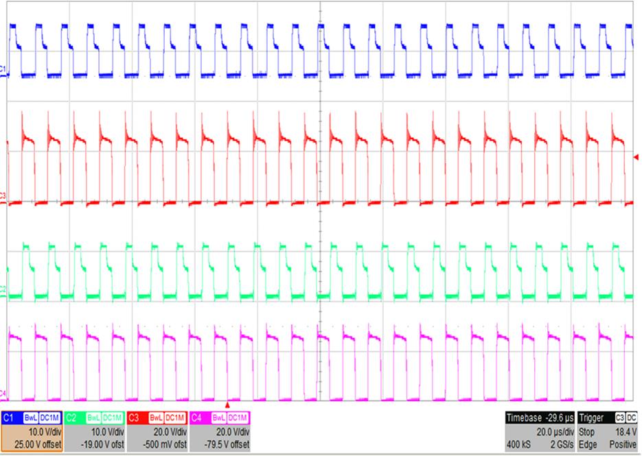 Figure 9-10 VIN = 410 V, IOUT = 10 A Full Load
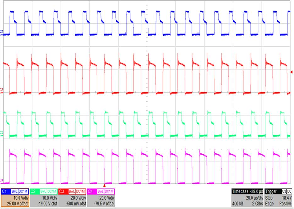 Figure 9-7 VIN = 390 V, IOUT = 10 A Full Load
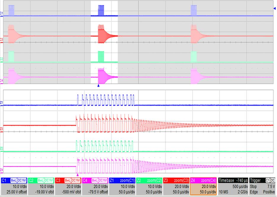 Figure 9-9 VIN = 410 V, IOUT = 0.3 A, LLC is Operating In Burst Mode
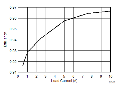 Figure 9-11 VIN = 390 V, Power Converter System Efficiency Using SR FETs