ZHCSGB1C March 2013 – December 2019 TPS84A20
PRODUCTION DATA.
- 1 特性
- 2 应用
- 3 说明
- 4 修订历史记录
- 5 Ordering Information
- 6 Specifications
- 7 Device Information
- 8 Typical Characteristics (PVIN = VIN = 12 V)
- 9 Typical Characteristics (PVIN = VIN = 5 V)
- 10Typical Characteristics (PVIN = 3.3 V, VIN = 5 V)
-
11Application Information
- 11.1 Adjusting the Output Voltage
- 11.2 Capacitor Recommendations for the TPS84A20 Power Supply
- 11.3 Transient Response
- 11.4 Transient Waveforms
- 11.5 Application Schematics
- 11.6 VIN and PVIN Input Voltage
- 11.7 3.3 V PVIN Operation
- 11.8 Power Good (PWRGD)
- 11.9 Light Load Efficiency (LLE)
- 11.10 SYNC_OUT
- 11.11 Parallel Operation
- 11.12 Power-Up Characteristics
- 11.13 Pre-Biased Start-Up
- 11.14 Remote Sense
- 11.15 Thermal Shutdown
- 11.16 Output On/Off Inhibit (INH)
- 11.17 Slow Start (SS/TR)
- 11.18 Overcurrent Protection
- 11.19 Synchronization (CLK)
- 11.20 Sequencing (SS/TR)
- 11.21 Programmable Undervoltage Lockout (UVLO)
- 11.22 Layout Considerations
- 11.23 EMI
- 12器件和文档支持
- 13机械、封装和可订购信息
8 Typical Characteristics (PVIN = VIN = 12 V)
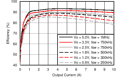 Figure 1. Efficiency versus Output Current
 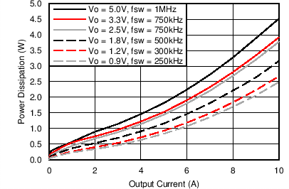 Figure 3. Power Dissipation versus Output Current
 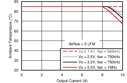 Figure 5. Safe Operating Area
 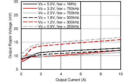 Figure 2. Voltage Ripple versus Output Current
 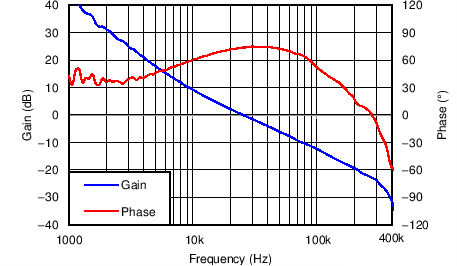 Figure 4. VOUT = 1.8 V, IOUT = 10 A, COUT1 = 200 µF Ceramic, fSW = 500 kHz
 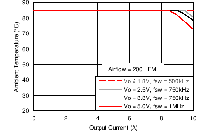 Figure 6. Safe Operating Area