ZHCSLB3B April 2020 – May 2025 TPS7B84-Q1
PRODUCTION DATA
- 1
- 1 特性
- 2 应用
- 3 说明
- 4 Pin Configuration and Functions
- 5 Specifications
- 6 Detailed Description
-
7 Application and Implementation
- 7.1 Application Information
- 7.2 Typical Application
- 7.3 Power Supply Recommendations
- 7.4 Layout
- 8 Device and Documentation Support
- 9 Revision History
- 10Mechanical, Packaging, and Orderable Information
封装选项
请参考 PDF 数据表获取器件具体的封装图。
机械数据 (封装 | 引脚)
- DCY|4
- DRB|8
散热焊盘机械数据 (封装 | 引脚)
- DRB|8
订购信息
6.3.4 Current Limit
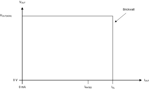
The device has an internal current limit circuit that protects the regulator during transient high-load current faults or shorting events. The current limit is a brickwall scheme. In a high-load current fault, the brickwall scheme limits the output current to the current limit (ICL). ICL is listed in the Electrical Characteristics table.
The output voltage is not regulated when the device is in current limit. When a current limit event occurs, the device begins to heat up because of the increase in power dissipation. When the device is in brickwall current limit, the pass transistor dissipates power [(VIN – VOUT) × ICL]. If thermal shutdown is triggered, the device turns off. After the device cools down, the internal thermal shutdown circuit turns the device back on. If the output current fault condition continues, the device cycles between current limit and thermal shutdown. For more information on current limits, see the Know Your Limits application report.
Figure 6-3 shows a diagram of the current limit.
 Figure 6-3 Current Limit