ZHCSQC5B December   2022  – February 2024 TPS7A21-Q1

PRODMIX  

  1.   1
  2. 特性
  3. 应用
  4. 说明
  5. Pin Configuration and Functions
  6. Specifications
    1. 5.1 Absolute Maximum Ratings
    2. 5.2 ESD Ratings
    3. 5.3 Recommended Operating Conditions
    4. 5.4 Thermal Information
    5. 5.5 Electrical Characteristics
    6. 5.6 Typical Characteristics
  7. Detailed Description
    1. 6.1 Overview
    2. 6.2 Functional Block Diagram
    3. 6.3 Feature Description
      1. 6.3.1 Smart Enable (EN)
      2. 6.3.2 Low Output Noise
      3. 6.3.3 Active Discharge
      4. 6.3.4 Dropout Voltage
      5. 6.3.5 Foldback Current Limit
      6. 6.3.6 Undervoltage Lockout
      7. 6.3.7 Thermal Overload Protection (TSD)
    4. 6.4 Device Functional Modes
      1. 6.4.1 Device Functional Mode Comparison
      2. 6.4.2 Normal Operation
      3. 6.4.3 Dropout Operation
      4. 6.4.4 Disabled
  8. Applications and Implementation
    1. 7.1 Application Information
      1. 7.1.1 Recommended Capacitor Types
      2. 7.1.2 Input and Output Capacitor Requirements
      3. 7.1.3 Load Transient Response
      4. 7.1.4 Undervoltage Lockout (UVLO) Operation
      5. 7.1.5 Power Dissipation (PD)
      6. 7.1.6 Estimating Junction Temperature
      7. 7.1.7 Recommended Area For Continuous Operation
    2. 7.2 Typical Application
      1. 7.2.1 Design Requirements
      2. 7.2.2 Detailed Design Procedure
        1. 7.2.2.1 Power Dissipation and Device Operation
      3. 7.2.3 Application Curves
    3. 7.3 Power Supply Recommendations
    4. 7.4 Layout
      1. 7.4.1 Layout Guidelines
      2. 7.4.2 Layout Example
  9. Device and Documentation Support
    1. 8.1 Device Support
      1. 8.1.1 Device Nomenclature
    2. 8.2 Documentation Support
      1. 8.2.1 Related Documentation
    3. 8.3 接收文档更新通知
    4. 8.4 支持资源
    5. 8.5 Trademarks
    6. 8.6 静电放电警告
    7. 8.7 术语表
  10. Revision History
  11. 10Mechanical, Packaging, and Orderable Information

封装选项

机械数据 (封装 | 引脚)
散热焊盘机械数据 (封装 | 引脚)
订购信息

Dropout Voltage

Dropout voltage (VDO) is defined as the input voltage minus the output voltage (VIN – VOUT) at the rated output current (IRATED), when the pass transistor is fully on. IRATED is the maximum IOUT listed in the Recommended Operating Conditions table. The pass transistor is in the ohmic or triode region of operation, and acts as a switch. The dropout voltage indirectly specifies a minimum input voltage greater than the nominal programmed output voltage at which the output voltage is expected to stay in regulation. If the input voltage falls to less than the value required to support output regulation, then the output voltage falls as well.

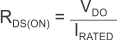
For a CMOS regulator, the dropout voltage is determined by the drain-source, on-state resistance (RDS(ON)) of the pass transistor. Therefore, if the linear regulator operates at less than the rated current, the dropout voltage for that current scales accordingly. Equation 1 calculates the RDS(ON) of the device.

Equation 1. GUID-B6D7C7D0-DEAD-427C-AE02-F343D9ADC013-low.gif