ZHCSD04E November 2014 – March 2022 TPS65400
PRODUCTION DATA
- 1 特性
- 2 应用
- 3 说明
- 4 Revision History
- 5 说明(续)
- 6 Pin Configuration and Functions
- 7 Specifications
-
8 Detailed Description
- 8.1 Overview
- 8.2 Functional Block Diagrams
- 8.3
Feature Description
- 8.3.1 Startup Timing and Power Sequencing
- 8.3.2 UVLO and Precision Enables
- 8.3.3 Soft-Start and Prebiased Startup
- 8.3.4 PWM Switching Frequency Selection
- 8.3.5 Clock Synchronization
- 8.3.6 Phase Interleaving
- 8.3.7 Fault Handling
- 8.3.8 OCP for SW1 to SW4
- 8.3.9 Overcurrent Protection for SW1 to SW4 in Current Sharing Operation
- 8.3.10 Recovery on Power Loss
- 8.3.11 Feedback Compensation
- 8.3.12 Adjusting Output Voltage
- 8.3.13 Digital Interface – PMBus
- 8.3.14 Initial Configuration
- 8.4 Device Functional Modes
- 8.5 Programming
- 8.6
Register Maps
- 8.6.1
PMBus Core Commands
- 8.6.1.1 (00h) PAGE
- 8.6.1.2 (01h) OPERATION
- 8.6.1.3 (03h) CLEAR_FAULTS
- 8.6.1.4 (10h) WRITE_PROTECT
- 8.6.1.5 (11h) STORE_DEFAULT_ALL
- 8.6.1.6 (19h) CAPABILITY
- 8.6.1.7 (78h) STATUS_BYTE
- 8.6.1.8 (79h) STATUS_WORD
- 8.6.1.9 (7Ah) STATUS_VOUT
- 8.6.1.10 (80h) STATUS_MFR_SPECIFIC
- 8.6.1.11 (98h) PMBUS_REVISION
- 8.6.1.12 (ADh) IC_DEVICE_ID
- 8.6.1.13 (AEh) IC_DEVICE_REV
- 8.6.2
Manufacturer-Specific Commands
- 8.6.2.1 (D0h) USER_DATA_BYTE_00
- 8.6.2.2 (D1h) USER_DATA_BYTE_01
- 8.6.2.3 (D2h) PIN_CONFIG_00
- 8.6.2.4 (D3h) PIN_CONFIG_01
- 8.6.2.5 (D4h) SEQUENCE_CONFIG
- 8.6.2.6 (D5h) SEQUENCE_ORDER
- 8.6.2.7 (D6h) IOUT_MODE
- 8.6.2.8 (D7h) FREQUENCY_PHASE
- 8.6.2.9 (D8h) VREF_COMMAND
- 8.6.2.10 (D9h) IOUT_MAX
- 8.6.2.11 (DAh) USER_RAM_00
- 8.6.2.12 (DBh) SOFT_RESET
- 8.6.2.13 (DCh) RESET_DELAY
- 8.6.2.14 (DDh) TON_TOFF_DELAY
- 8.6.2.15 (DEh) TON_TRANSITION_RATE
- 8.6.2.16 (DFh) VREF_TRANSITION_RATE
- 8.6.2.17 (F0h) SLOPE_COMPENSATION
- 8.6.2.18 (F1h) ISENSE_GAIN
- 8.6.2.19 (FCh) DEVICE_CODE
- 8.6.1
PMBus Core Commands
- 9 Application and Implementation
- 10Power Supply Recommendations
- 11Layout
- 12Device and Documentation Support
- 13Mechanical, Packaging, and Orderable Information
8.3.4 PWM Switching Frequency Selection
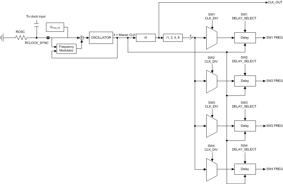
The master clock frequency, FOSC, can be set by external resistor on the RCLOCK_SYNC terminal, or by synchronizing with an external clock. To set using an external resistor, use this formula.
 Figure 8-8 Frequency vs Rosc
To sync to an external source, an AC-coupled signal should be applied to the terminal. A fixed resistor should still be connected to set a minimum frequency. The frequency of the input signal to synchronize with should always be higher than the minimum frequency. If the internal PLL cannot synchronize, the switchers will fall back to the minimum frequency set by the resistor. The CLK_OUT terminal outputs the master clock FOSC.
The PWM frequency of each switcher is determined by this master clock frequency and an I2C-programmable choice of 4 divider ratios (1, 2, 4, or 8) by setting CLK_DIV (see (D7h) FREQUENCY_PHASE).

The intent of the individual divider ratios is to allow users to set the frequency of each switcher independently. For example, with a master clock FOSC of 1.1 MHz, SW1 and SW2 have a divider ratio of 4 for a 275-kHz PWM, and SW3 and SW4 have a divider ratio of 1 for a PWM frequency of 1.1 MHz. Select the divider ratio so that the PWM frequency stays within the range of 275 kHz to 2.2 MHz for whichever master clock frequency is set.
In addition to selecting the frequency, each switcher can have its PWM frequency delayed. This enables the designer to minimize ripple current by properly selecting the delays so that the switching frequencies are out of phase. The default switching frequency is at CLK_DIV = FOSC / 1 with PHASE_DELAY for SW1 at 0°, SW2 at 180°, SW3 at 90°, and SW4 at 270°. More information on frequency selection and delay is given in (D7h) FREQUENCY_PHASE.