ZHCSD04E November 2014 – March 2022 TPS65400
PRODUCTION DATA
- 1 特性
- 2 应用
- 3 说明
- 4 Revision History
- 5 说明(续)
- 6 Pin Configuration and Functions
- 7 Specifications
-
8 Detailed Description
- 8.1 Overview
- 8.2 Functional Block Diagrams
- 8.3
Feature Description
- 8.3.1 Startup Timing and Power Sequencing
- 8.3.2 UVLO and Precision Enables
- 8.3.3 Soft-Start and Prebiased Startup
- 8.3.4 PWM Switching Frequency Selection
- 8.3.5 Clock Synchronization
- 8.3.6 Phase Interleaving
- 8.3.7 Fault Handling
- 8.3.8 OCP for SW1 to SW4
- 8.3.9 Overcurrent Protection for SW1 to SW4 in Current Sharing Operation
- 8.3.10 Recovery on Power Loss
- 8.3.11 Feedback Compensation
- 8.3.12 Adjusting Output Voltage
- 8.3.13 Digital Interface – PMBus
- 8.3.14 Initial Configuration
- 8.4 Device Functional Modes
- 8.5 Programming
- 8.6
Register Maps
- 8.6.1
PMBus Core Commands
- 8.6.1.1 (00h) PAGE
- 8.6.1.2 (01h) OPERATION
- 8.6.1.3 (03h) CLEAR_FAULTS
- 8.6.1.4 (10h) WRITE_PROTECT
- 8.6.1.5 (11h) STORE_DEFAULT_ALL
- 8.6.1.6 (19h) CAPABILITY
- 8.6.1.7 (78h) STATUS_BYTE
- 8.6.1.8 (79h) STATUS_WORD
- 8.6.1.9 (7Ah) STATUS_VOUT
- 8.6.1.10 (80h) STATUS_MFR_SPECIFIC
- 8.6.1.11 (98h) PMBUS_REVISION
- 8.6.1.12 (ADh) IC_DEVICE_ID
- 8.6.1.13 (AEh) IC_DEVICE_REV
- 8.6.2
Manufacturer-Specific Commands
- 8.6.2.1 (D0h) USER_DATA_BYTE_00
- 8.6.2.2 (D1h) USER_DATA_BYTE_01
- 8.6.2.3 (D2h) PIN_CONFIG_00
- 8.6.2.4 (D3h) PIN_CONFIG_01
- 8.6.2.5 (D4h) SEQUENCE_CONFIG
- 8.6.2.6 (D5h) SEQUENCE_ORDER
- 8.6.2.7 (D6h) IOUT_MODE
- 8.6.2.8 (D7h) FREQUENCY_PHASE
- 8.6.2.9 (D8h) VREF_COMMAND
- 8.6.2.10 (D9h) IOUT_MAX
- 8.6.2.11 (DAh) USER_RAM_00
- 8.6.2.12 (DBh) SOFT_RESET
- 8.6.2.13 (DCh) RESET_DELAY
- 8.6.2.14 (DDh) TON_TOFF_DELAY
- 8.6.2.15 (DEh) TON_TRANSITION_RATE
- 8.6.2.16 (DFh) VREF_TRANSITION_RATE
- 8.6.2.17 (F0h) SLOPE_COMPENSATION
- 8.6.2.18 (F1h) ISENSE_GAIN
- 8.6.2.19 (FCh) DEVICE_CODE
- 8.6.1
PMBus Core Commands
- 9 Application and Implementation
- 10Power Supply Recommendations
- 11Layout
- 12Device and Documentation Support
- 13Mechanical, Packaging, and Orderable Information
8.3.8 OCP for SW1 to SW4
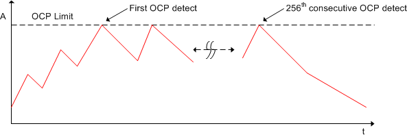
The OCP is I2C-programmable and set by the IOUT_MAX command. By default, the peak current IOUT_MAX for SW1 and SW2 is 6 A, and for SW3 and SW4 it is 3 A. When the current reaches this threshold, the unit immediately turns off the high-side FET and keeps the low-side FET off for the remainder of the switching cycle. The following cycle are skipped (high-side FET off, low-side FET off) regardless of the inductor current. If the current in the inductor is still higher than the IOUT_MAX after the skipped cycle, the following cycles are also skipped until the current reach below the IOUT_MAX.
If the IOUT_MAX is reached more than 256 active cycles continuously, the switcher shut downs for 20 ms and restarts. If the switcher is running in interleaved operation, both the switcher that tripped the IOUT_MAX threshold and its interleaved counterpart shut down for 20 ms. After that period of time, the unit restarts and goes through soft-start operation. For very-low duty cycle operation and faulty operation with very-fast current increase during the high-side FET on-time (due to inductor saturation and so forth), OCP is also enforced on the low side to ensure no runaway condition exists.
| SWITCHER | IOUT_MAX |
|---|---|
| SW1, SW2 | 2 A |
| 3 A | |
| 4 A | |
| 5 A | |
| 6 A (default) | |
| SW3, SW4 | 0.5 A |
| 1 A | |
| 2 A | |
| 3 A (default) |
While the converter is shut down following an OCP event spanning more than 256 cycles, the COMP terminal is pulled low for 1.1 ms prior to precharge and re-enabling of the converter. At the same time, the SSx pin is discharged to AGND for 1.1 ms. If the soft-start is digital (SSx pins used as PGOODx outputs), the soft-start value is reset.
 Figure 8-11 Inductor Current During Overcurrent Event
At high switching frequency (>1 MHz) and particularly when there is a fault in the converter such as saturation of the inductor, the current sensor might not sense the overcurrent event. To ensure that current protection is provided in all operating scenarios, low-side current sensing is also present to provide overcurrent detection and protection when the low-side FET is on. If over-current is detected when the low-side FET is on, the low-side FET stays on (and the high-side FET off) until the current drops below the threshold. A new cycle will then begin (high side on, low side off) when the next switching cycle occurs as driven by the internal clock derived from the oscillator (internal or external synchronization). A dedicated counter records the low-side OCP events and initiates a shutdown of the converter after 256 OCP event counts. Six consecutive cycles without a low-side OCP event resets the counter.
 Figure 8-12 Inductor Current During Overcurrent Event With Low-Side Detection