ZHCSNP9B March 2021 – October 2021 TPS61379-Q1
PRODUCTION DATA
- 1 特性
- 2 应用
- 3 说明
- 4 Revision History
- 5 Device Comparison Table
- 6 Pin Configuration and Functions
- 7 Specifications
-
8 Detailed Description
- 8.1 Overview
- 8.2 Functional Block Diagrams
- 8.3
Feature Description
- 8.3.1 VCC Power Supply
- 8.3.2 Input Undervoltage Lockout (UVLO)
- 8.3.3 Enable and Soft Start
- 8.3.4 Shut Down
- 8.3.5 Switching Frequency Setting
- 8.3.6 Spread Spectrum Frequency Modulation
- 8.3.7 Bootstrap
- 8.3.8 Load Disconnect
- 8.3.9 MODE/SYNC Configuration
- 8.3.10 Overvoltage Protection (OVP)
- 8.3.11 Output Short Protection/Hiccup
- 8.3.12 Power-Good Indicator
- 8.3.13 Thermal Shutdown
- 8.4 Device Functional Modes
-
9 Application and Implementation
- 9.1 Application Information
- 9.2
Typical Application
- 9.2.1 Design Requirements
- 9.2.2 Detailed Design Procedure
- 9.2.3 Application Curves
- 10Power Supply Recommendations
- 11Layout
- 12Device and Documentation Support
- 13Mechanical, Packaging, and Orderable Information
9.2.2.4 Selecting the Output Capacitors
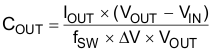
The output capacitor is mainly selected to meet the requirements at load transient or steady state. Then the loop is compensated for the output capacitor selected. The output ripple voltage is related to the equivalent series resistance (ESR) of the capacitor and its capacitance. Assuming a capacitor with zero ESR, the minimum capacitance needed for a given ripple can be calculated by Equation 10:
where
- COUT is the output capacitor
- IOUT is the output current
- VOUT is the output voltage
- VIN is the input voltage
- ΔV is the output voltage ripple required
- ƒSW is the switching frequency
The additional output ripple component caused by ESR is calculated by Equation 11:

where
- ΔVESR is the output voltage ripple caused by ESR
- RESR is the resistor in series with the output capacitor
For the ceramic capacitor, the ESR ripple can be neglected. However, for tantalum or electrolytic capacitors, it must be considered if used.
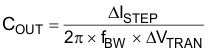
The minimum ceramic output capacitance needed to meet a load transient requirement can be estimated using Equation 12:
where
- ΔISTEP is the transient load current step
- ΔVTRAN is the allowed voltage dip for the load current step
- ƒBW is the control loop bandwidth (that is, the frequency where the control loop gain crosses zero)
For the output capacitor on the OUT pin, the effective capacitance is recommended between 0.22 μF to 1 μF.
Care must be taken when evaluating the derating of a ceramic capacitor under the DC bias. Ceramic capacitors can derate by as much as 70% of its capacitance at its rated voltage. Therefore, enough margins on the voltage rating must be considered to ensure adequate capacitance at the required output voltage.