ZHCS901E May 2012 – September 2021 TPS55340
PRODUCTION DATA
- 1 特性
- 2 应用
- 3 说明
- 4 Revision History
- 5 Pin Configuration and Functions
- 6 Specifications
- 7 Detailed Description
-
8 Application and Implementation
- 8.1 Application Information
- 8.2
Typical Applications
- 8.2.1
Boost Converter
- 8.2.1.1 Design Requirements
- 8.2.1.2
Detailed Design Procedure
- 8.2.1.2.1 Custom Design with WEBENCH Tools
- 8.2.1.2.2 Selecting the Switching Frequency (R4)
- 8.2.1.2.3 Determining the Duty Cycle
- 8.2.1.2.4 Selecting the Inductor (L1)
- 8.2.1.2.5 Computing the Maximum Output Current
- 8.2.1.2.6 Selecting the Output Capacitors (C8, C9, C10)
- 8.2.1.2.7 Selecting the Input Capacitors (C2, C7)
- 8.2.1.2.8 Setting Output Voltage (R1, R2)
- 8.2.1.2.9 Setting the Soft-start Time (C7)
- 8.2.1.2.10 Selecting the Schottky Diode (D1)
- 8.2.1.2.11 Compensating the Control Loop (R3, C4, C5)
- 8.2.1.3 Application Curves
- 8.2.2
SEPIC Converter
- 8.2.2.1 Design Requirements
- 8.2.2.2
Detailed Design Procedure
- 8.2.2.2.1 Selecting the Switching Frequency (R4)
- 8.2.2.2.2 Duty Cycle
- 8.2.2.2.3 Selecting the Inductor (L1)
- 8.2.2.2.4 Calculating the Maximum Output Current
- 8.2.2.2.5 Selecting the Output Capacitors (C8, C9, C10)
- 8.2.2.2.6 Selecting the Series Capacitor (C6)
- 8.2.2.2.7 Selecting the Input Capacitor (C2, C7)
- 8.2.2.2.8 Selecting the Schottky Diode (D1)
- 8.2.2.2.9 Setting the Output Voltage (R1, R2)
- 8.2.2.2.10 Setting the Soft-start Time (C3)
- 8.2.2.2.11 MOSFET Rating Considerations
- 8.2.2.2.12 Compensating the Control Loop (R3, C4)
- 8.2.2.3 Application Curves
- 8.2.1
Boost Converter
- 9 Power Supply Recommendations
- 10Layout
- 11Device and Documentation Support
- 12Mechanical, Packaging, and Orderable Information
封装选项
机械数据 (封装 | 引脚)
散热焊盘机械数据 (封装 | 引脚)
订购信息
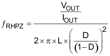
8.2.2.2.12 Compensating the Control Loop (R3, C4)
This design was compensated by measuring the frequency response of the power stage at the lowest input voltage of 6 V and choosing the components for the desired bandwidth. The lowest right half plane zero (ƒRHPZ) is calculated to be 36.7 kHz with Equation 52. Using the recommendation to limit the bandwidth to 1/3 of ƒRHPZ, the maximum recommended is 12.2 kHz.
This design also uses only one pole and one zero. To achieve approximately 60 degrees of phase margin, the power stage phase must be no lower than approximately –120 degrees at the desired bandwidth. To ensure a stable design, R3 was initially set to 1 kΩ and C4 was 1 µF. Figure 8-11 shows the measurement of the power stage. At 7 kHz the power stage has a gain of 19.52 dB and phase of –118.1 degrees.
 Figure 8-11 SEPIC Power Stage Gain and Phase
As there are no changes in the transconductance amplifier, the equations used to calculate the external compensation components in a boost design can be used in the SEPIC design. Using the maximum Gea from the electrical specification of 440 µmho, Equation 38 calculates the nearest standard value of R3 to be 2.37 kΩ. Using Equation 39, C4 is calculated to the nearest standard value of 0.1 µF.