ZHCS901E May 2012 – September 2021 TPS55340
PRODUCTION DATA
- 1 特性
- 2 应用
- 3 说明
- 4 Revision History
- 5 Pin Configuration and Functions
- 6 Specifications
- 7 Detailed Description
-
8 Application and Implementation
- 8.1 Application Information
- 8.2
Typical Applications
- 8.2.1
Boost Converter
- 8.2.1.1 Design Requirements
- 8.2.1.2
Detailed Design Procedure
- 8.2.1.2.1 Custom Design with WEBENCH Tools
- 8.2.1.2.2 Selecting the Switching Frequency (R4)
- 8.2.1.2.3 Determining the Duty Cycle
- 8.2.1.2.4 Selecting the Inductor (L1)
- 8.2.1.2.5 Computing the Maximum Output Current
- 8.2.1.2.6 Selecting the Output Capacitors (C8, C9, C10)
- 8.2.1.2.7 Selecting the Input Capacitors (C2, C7)
- 8.2.1.2.8 Setting Output Voltage (R1, R2)
- 8.2.1.2.9 Setting the Soft-start Time (C7)
- 8.2.1.2.10 Selecting the Schottky Diode (D1)
- 8.2.1.2.11 Compensating the Control Loop (R3, C4, C5)
- 8.2.1.3 Application Curves
- 8.2.2
SEPIC Converter
- 8.2.2.1 Design Requirements
- 8.2.2.2
Detailed Design Procedure
- 8.2.2.2.1 Selecting the Switching Frequency (R4)
- 8.2.2.2.2 Duty Cycle
- 8.2.2.2.3 Selecting the Inductor (L1)
- 8.2.2.2.4 Calculating the Maximum Output Current
- 8.2.2.2.5 Selecting the Output Capacitors (C8, C9, C10)
- 8.2.2.2.6 Selecting the Series Capacitor (C6)
- 8.2.2.2.7 Selecting the Input Capacitor (C2, C7)
- 8.2.2.2.8 Selecting the Schottky Diode (D1)
- 8.2.2.2.9 Setting the Output Voltage (R1, R2)
- 8.2.2.2.10 Setting the Soft-start Time (C3)
- 8.2.2.2.11 MOSFET Rating Considerations
- 8.2.2.2.12 Compensating the Control Loop (R3, C4)
- 8.2.2.3 Application Curves
- 8.2.1
Boost Converter
- 9 Power Supply Recommendations
- 10Layout
- 11Device and Documentation Support
- 12Mechanical, Packaging, and Orderable Information
封装选项
机械数据 (封装 | 引脚)
散热焊盘机械数据 (封装 | 引脚)
订购信息
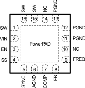
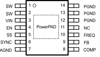
5 Pin Configuration and Functions

TI recommends
connecting NC with AGND.
Figure 5-1 RTE Package16-Pin WQFNTop View
TI recommends
connecting NC with AGND.
Figure 5-2 PWP Package14-Pin HTSSOP(Top View)Table 5-1 Pin Functions
| PIN | DESCRIPTION | ||
|---|---|---|---|
| NAME | QFN-16 | HTSSOP-14 | |
| AGND | 6 | 7 | Signal ground of the IC |
| COMP | 7 | 8 | Output of the transconductance error amplifier. An external RC network connected to this pin compensates the regulator feedback loop. |
| EN | 3 | 4 | Enable pin. When the voltage of this pin falls below the enable threshold for more than 1 ms, the IC turns off. |
| FB | 8 | 9 | Error amplifier input and feedback pin for positive voltage regulation. Connect to the center tap of a resistor divider to program the output voltage. |
| FREQ | 9 | 10 | Switching frequency program pin. An external resistor connected between the FREQ pin and AGND sets the switching frequency. |
| NC | 10, 14 | 11 | Reserved pin that must be connected to ground |
| PGND | 11, 12, 13 | 12, 13, 14 | Power ground of the IC. It is connected to the source of the internal power MOSFET switch. |
| PowerPAD | — | — | The PowerPAD should be soldered to the AGND. If possible, use thermal vias to connect to internal ground plane for improved power dissipation. |
| SS | 4 | 5 | Soft-start programming pin. A capacitor between the SS pin and AGND pin programs soft-start timing. |
| SW | 1, 15, 16 | 1, 2 | SW is the drain of the internal power MOSFET. Connect SW to the switched side of the boost or SEPIC inductor or the flyback transformer. |
| SYNC | 5 | 6 | Switching frequency synchronization pin. An external clock signal can be used to set the switching frequency between 200 kHz and 1.0 MHz. If not used, this pin should be tied to AGND. |
| VIN | 2 | 3 | The input supply pin to the IC. Connect VIN to a supply voltage between 2.9 V and 32 V. It is acceptable for the voltage on the pin to be different from the boost power stage input. |