ZHCS901E May 2012 – September 2021 TPS55340
PRODUCTION DATA
- 1 特性
- 2 应用
- 3 说明
- 4 Revision History
- 5 Pin Configuration and Functions
- 6 Specifications
- 7 Detailed Description
-
8 Application and Implementation
- 8.1 Application Information
- 8.2
Typical Applications
- 8.2.1
Boost Converter
- 8.2.1.1 Design Requirements
- 8.2.1.2
Detailed Design Procedure
- 8.2.1.2.1 Custom Design with WEBENCH Tools
- 8.2.1.2.2 Selecting the Switching Frequency (R4)
- 8.2.1.2.3 Determining the Duty Cycle
- 8.2.1.2.4 Selecting the Inductor (L1)
- 8.2.1.2.5 Computing the Maximum Output Current
- 8.2.1.2.6 Selecting the Output Capacitors (C8, C9, C10)
- 8.2.1.2.7 Selecting the Input Capacitors (C2, C7)
- 8.2.1.2.8 Setting Output Voltage (R1, R2)
- 8.2.1.2.9 Setting the Soft-start Time (C7)
- 8.2.1.2.10 Selecting the Schottky Diode (D1)
- 8.2.1.2.11 Compensating the Control Loop (R3, C4, C5)
- 8.2.1.3 Application Curves
- 8.2.2
SEPIC Converter
- 8.2.2.1 Design Requirements
- 8.2.2.2
Detailed Design Procedure
- 8.2.2.2.1 Selecting the Switching Frequency (R4)
- 8.2.2.2.2 Duty Cycle
- 8.2.2.2.3 Selecting the Inductor (L1)
- 8.2.2.2.4 Calculating the Maximum Output Current
- 8.2.2.2.5 Selecting the Output Capacitors (C8, C9, C10)
- 8.2.2.2.6 Selecting the Series Capacitor (C6)
- 8.2.2.2.7 Selecting the Input Capacitor (C2, C7)
- 8.2.2.2.8 Selecting the Schottky Diode (D1)
- 8.2.2.2.9 Setting the Output Voltage (R1, R2)
- 8.2.2.2.10 Setting the Soft-start Time (C3)
- 8.2.2.2.11 MOSFET Rating Considerations
- 8.2.2.2.12 Compensating the Control Loop (R3, C4)
- 8.2.2.3 Application Curves
- 8.2.1
Boost Converter
- 9 Power Supply Recommendations
- 10Layout
- 11Device and Documentation Support
- 12Mechanical, Packaging, and Orderable Information
封装选项
机械数据 (封装 | 引脚)
散热焊盘机械数据 (封装 | 引脚)
订购信息
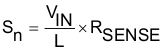
7.3.6 Slope Compensation
The TPS55340 has internal slope compensation to prevent subharmonic oscillations. The sensed current slope of boost converter can be expressed as Equation 4:
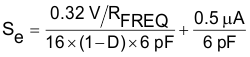
The slope compensation dv/dt can be calculated using Equation 5.
In a converter with current mode control, in addition to the output voltage feedback loop, the inner current loop including the inductor current sampling effect as well as the slope compensation on the small signal response should be taken into account, which can be modeled as seen in Equation 6:
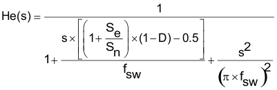
where
- RSENSE (15 mΩ) is the equivalent current sense resistor.
- RFREQ is timing resistor used to set frequency.
- D is the duty cycle.
If Sn << Se, the converter operates in voltage mode control rather than current mode control, and Equation 6 is no longer valid.