ZHCSAL1F November 2010 – May 2019 TPS54618
PRODUCTION DATA.
- 1 特性
- 2 应用
- 3 说明
- 4 修订历史记录
- 5 Pin Configuration and Functions
- 6 Specifications
-
7 Detailed Description
- 7.1 Overview
- 7.2 Functional Block Diagram
- 7.3
Feature Description
- 7.3.1 Fixed Frequency PWM Control
- 7.3.2 Slope Compensation and Output Current
- 7.3.3 Bootstrap Voltage (Boot) and Low Dropout Operation
- 7.3.4 Error Amplifier
- 7.3.5 Voltage Reference
- 7.3.6 Adjusting the Output Voltage
- 7.3.7 Enable and Adjusting Undervoltage Lockout
- 7.3.8 Soft-Start Pin
- 7.3.9 Sequencing
- 7.3.10 Constant Switching Frequency and Timing Resistor (RT/CLK Pin)
- 7.3.11 Overcurrent Protection
- 7.3.12 Frequency Shift
- 7.3.13 Reverse Overcurrent Protection
- 7.3.14 Synchronize Using the RT/CLK Pin
- 7.3.15 Power Good (PWRGD Pin)
- 7.3.16 Overvoltage Transient Protection
- 7.3.17 Thermal Shutdown
- 7.4 Device Functional Modes
-
8 Application and Implementation
- 8.1 Application Information
- 8.2
Typical Application
- 8.2.1 Design Requirements
- 8.2.2
Detailed Design Procedure
- 8.2.2.1 Custom Design With WEBENCH® Tools
- 8.2.2.2 Step One: Select the Switching Frequency
- 8.2.2.3 Step Two: Select the Output Inductor
- 8.2.2.4 Step Three: Choose the Output Capacitor
- 8.2.2.5 Step Four: Select the Input Capacitor
- 8.2.2.6 Step Five: Choose the Soft-Start Capacitor
- 8.2.2.7 Step Six: Select the Bootstrap Capacitor
- 8.2.2.8 Step Eight: Select Output Voltage and Feedback Resistors
- 8.2.2.9 Step Nine: Select Loop Compensation Components
- 8.2.3 Application Curves
- 9 Power Supply Recommendations
- 10Layout
- 11器件和文档支持
- 12机械、封装和可订购信息
7.3.14 Synchronize Using the RT/CLK Pin
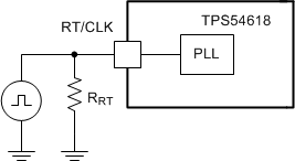
The RT/CLK pin is used to synchronize the converter to an external system clock. See Figure 33. To implement the synchronization feature in a system, connect a square wave to the RT/CLK pin with an ON-time of at least
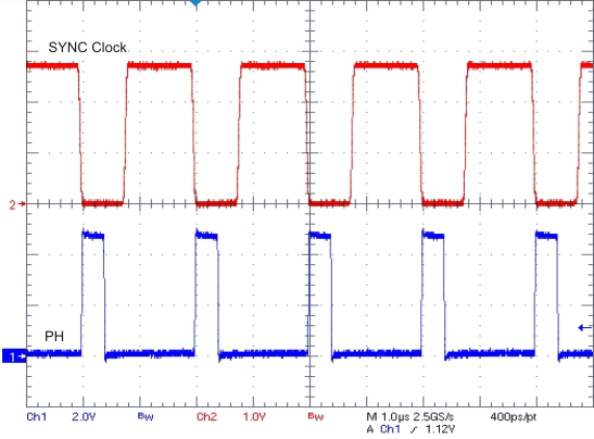
75 ns. If the pin is pulled above the PLL upper threshold, a mode change occurs and the pin becomes a synchronization input. The internal amplifier is disabled and the pin is a high impedance clock input to the internal PLL. If clocking edges stop, the internal amplifier is re-enabled and the mode returns to the frequency set by the resistor. The square wave amplitude at this pin must transition lower than 0.6 V and higher than 1.6 V typically. The synchronization frequency range is 300 kHz to 2000 kHz. The rising edge of the PH is synchronized to the falling edge of RT/CLK pin.
 Figure 33. Synchronizing to a System Clock
  Figure 34. Plot of Synchronizing to System Clock