ZHCSQ76 December   2022 TPS25961

PRODUCTION DATA  

  1. 特性
  2. 应用
  3. 说明
  4. Revision History
  5. Pin Configuration and Functions
  6. Specifications
    1. 6.1 Absolute Maximum Ratings
    2. 6.2 ESD Ratings
    3. 6.3 Recommended Operating Conditions
    4. 6.4 Thermal Information
    5. 6.5 Electrical Characteristics
    6. 6.6 Timing Requirements
    7. 6.7 Switching Characteristics
    8. 6.8 典型特性
  7. Detailed Description
    1. 7.1 Overview
    2. 7.2 Functional Block Diagram
    3. 7.3 Feature Description
      1. 7.3.1 欠压保护 (UVP) 和欠压锁定 (UVLO)
      2. 7.3.2 Overvoltage Protection
      3. 7.3.3 Inrush Current, Overcurrent and Short Circuit Protection
        1. 7.3.3.1 Slew Rate and Inrush Current Control (dVdt)
        2. 7.3.3.2 Active Current Limiting
        3. 7.3.3.3 Short-Circuit Protection
      4. 7.3.4 Overtemperature Protection (OTP)
      5. 7.3.5 Fault Response
    4. 7.4 Device Functional Modes
  8. Application and Implementation
    1. 8.1 Application Information
    2. 8.2 典型应用
      1. 8.2.1 Adapter input protection for set-top boxes
      2. 8.2.2 Design Requirements
      3. 8.2.3 Detailed Design Procedure
        1. 8.2.3.1 Programming the Current-Limit Threshold: RILM Selection
        2. 8.2.3.2 欠压和过压锁定设定点
        3. 8.2.3.3 Output Voltage Rise Time (tR)
      4. 8.2.4 Application Curves
    3. 8.3 Application Example
      1. 8.3.1 Application Curves
    4. 8.4 Power Supply Recommendations
      1. 8.4.1 瞬态保护
      2. 8.4.2 Output Short-Circuit Measurements
    5. 8.5 Layout
      1. 8.5.1 Layout Guidelines
      2. 8.5.2 Layout Example
  9. Device and Documentation Support
    1. 9.1 Documentation Support
      1. 9.1.1 Related Documentation
    2. 9.2 接收文档更新通知
    3. 9.3 支持资源
    4. 9.4 商标
    5. 9.5 Electrostatic Discharge Caution
    6. 9.6 术语表
  10. 10Mechanical, Packaging, and Orderable Information

封装选项

机械数据 (封装 | 引脚)
散热焊盘机械数据 (封装 | 引脚)
订购信息

Overvoltage Protection

The TPS25961 implements Overvoltage Protection on VIN in case the applied voltage becomes too high for the system or device to properly operate. The Overvoltage Protection has a default lockout threshold of VOVP, which is achieved by connecting the OVLO pin to GND.
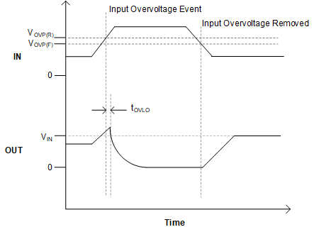
GUID-20220623-SS0I-1555-BXXV-TV4BVTGQJX5Q-low.gif Figure 7-2 TPS25961 Fixed Overvoltage Lockout Response

It’s possible to override the default OVLO threshold and adjust it to an user defined value as per the system requirements. This can be achieved by dividing the input supply and feeding it to the OVLO pin. Whenever the voltage at the OVLO pin rises above a threshold VOVLO(R), the device turns OFF the FET. When the voltage at the OVLO pin falls below the threshold VOVLO(F), the FET is turned ON again. The rising and falling thresholds on this pin are slightly different, thereby providing some hysteresis and ensuring stable operation around the threshold voltage.
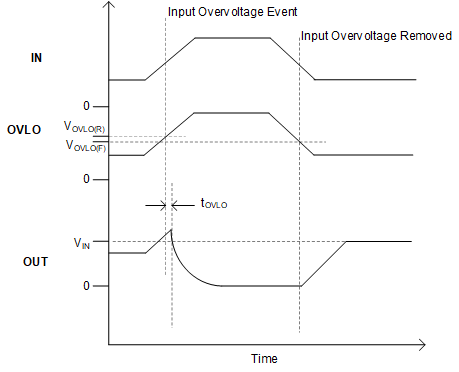
GUID-20220623-SS0I-0FRV-0ZPW-4RJWLD057RQW-low.gif Figure 7-3 TPS25961 Adjustable Overvoltage Lockout Response

The user should choose the resistor divider values appropriately to map the desired input overvoltage level to the OVLO threshold of the part.
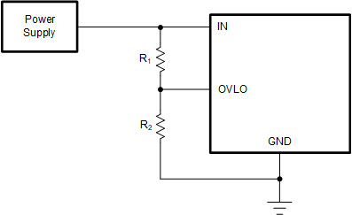
GUID-20220623-SS0I-MTRX-5HHD-3SGXK3MBM0XB-low.gif Figure 7-4 TPS25961 Adjustable Overvoltage Lockout
The equation below shows the calculations for the resistor divider values to be used to set the OVLO set-point for a given voltage supply.
Equation 2. VIN(OV)  = VOVLO(F) × R1 + R2R2