ZHCSP56 September   2023 TPS1HTC30-Q1

PRODUCTION DATA  

  1.   1
  2. 特性
  3. 应用
  4. 说明
  5. Revision History
  6. Pin Configuration and Functions
    1. 5.1 Recommended Connections for Unused Pins
  7. Specifications
    1. 6.1 Absolute Maximum Ratings
    2. 6.2 ESD Ratings
    3. 6.3 Recommended Operating Conditions
    4. 6.4 Thermal Information
    5. 6.5 Electrical Characteristics
    6. 6.6 SNS Timing Characteristics
    7. 6.7 Switching Characteristics
    8. 6.8 Timing Diagrams
    9. 6.9 Typical Characteristics
  8. Parameter Measurement Information
  9. Detailed Description
    1. 8.1 Overview
    2. 8.2 功能方框图
    3. 8.3 Feature Description
      1. 8.3.1 Accurate Current Sense
      2. 8.3.2 Programmable Current Limit
        1. 8.3.2.1 Capacitive Charging
      3. 8.3.3 Inductive-Load Switching-Off Clamp
      4. 8.3.4 Inductive Load Demagnetization
      5. 8.3.5 Full Protections and Diagnostics
        1. 8.3.5.1 Short-Circuit and Overload Protection
        2. 8.3.5.2 Open-Load Detection
        3. 8.3.5.3 Thermal Protection Behavior
        4. 8.3.5.4 Overvoltage (OVP) Protection
        5. 8.3.5.5 UVLO Protection
        6. 8.3.5.6 Reverse Polarity Protection
        7. 8.3.5.7 Protection for MCU I/Os
      6. 8.3.6 Diagnostic Enable Function
    4. 8.4 Device Functional Modes
      1. 8.4.1 Working Mode
  10. Application and Implementation
    1. 9.1 Application Information
    2. 9.2 Typical Application
      1. 9.2.1 Design Requirements
      2. 9.2.2 Detailed Design Procedure
        1. 9.2.2.1 Dynamically Changing Current Limit
      3. 9.2.3 Application Curves
    3. 9.3 Power Supply Recommendations
    4. 9.4 Layout
      1. 9.4.1 Layout Guidelines
      2. 9.4.2 Layout Example
        1. 9.4.2.1 Without a GND Network
        2. 9.4.2.2 With a GND Network
        3. 9.4.2.3 Thermal Considerations
  11. 10Device and Documentation Support
    1. 10.1 Documentation Support
      1. 10.1.1 Related Documentation
    2. 10.2 接收文档更新通知
    3. 10.3 支持资源
    4. 10.4 Trademarks
    5. 10.5 静电放电警告
    6. 10.6 术语表
  12. 11Mechanical, Packaging, and Orderable Information

封装选项

机械数据 (封装 | 引脚)
散热焊盘机械数据 (封装 | 引脚)
订购信息

Inductive Load Demagnetization

When switching off an inductive load, the inductor can impose a negative voltage on the output of the switch. The TPS1HTC30 includes voltage clamps between VS and VOUT to limit the voltage across the FETs and demagnetize load inductance if there is any. The negative voltage applied at the OUT pin drives the discharge of inductor current. Figure 8-6 shows the device discharging a 400-mH load.
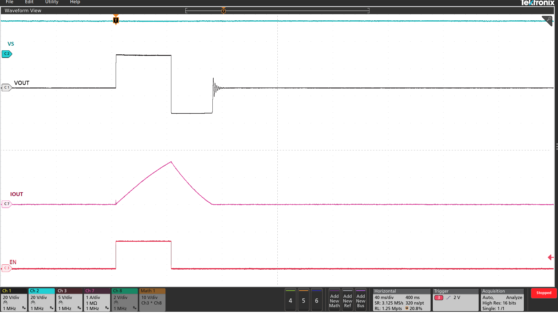
GUID-20221219-SS0I-PXQK-GQ8T-F4RWJSP14LHR-low.png Figure 8-6 TPS1HTC30 Inductive Discharge (400 mH)

The maximum acceptable load inductance is a function of the energy dissipated in the device and therefore the load current and the inductive load. The maximum energy and the load inductance the device can withstand for one pulse inductive dissipation at 125°C is shown in Figure 8-7. The device can withstand 50% of this energy for one million inductive repetitive pulses with a >4-Hz repetitive pulse. If the application parameters exceed this device limit, use a protection device like a freewheeling diode to dissipate the energy stored in the inductor.

GUID-20221221-SS0I-8CJT-X3ZF-XWN3LZBRJZHG-low.svg Figure 8-7 TPS1HTC30 Inductive Load Discharge Energy Capability at 125°C