ZHCSP75A July 2022 – December 2022 TPS1HC30-Q1
PRODUCTION DATA
- 1 特性
- 2 应用
- 3 说明
- 4 Revision History
- 5 Pin Configuration and Functions
- 6 Specifications
- 7 Parameter Measurement Information
-
8 Detailed Description
- 8.1 Overview
- 8.2 Functional Block Diagram
- 8.3
Feature Description
- 8.3.1 Accurate Current Sense
- 8.3.2 Programmable Current Limit
- 8.3.3 Inductive-Load Switching-Off Clamp
- 8.3.4
Full Protections and Diagnostics
- 8.3.4.1 Short-Circuit and Overload Protection
- 8.3.4.2 Open-Load and Short-to-Battery Detection
- 8.3.4.3 Short-to-Battery Detection
- 8.3.4.4 Reverse-Polarity and Battery Protection
- 8.3.4.5 Latch-Off Mode
- 8.3.4.6 Thermal Protection Behavior
- 8.3.4.7 UVLO Protection
- 8.3.4.8 Loss of GND Protection
- 8.3.4.9 Loss of Power Supply Protection
- 8.3.4.10 Reverse Current Protection
- 8.3.4.11 Protection for MCU I/Os
- 8.3.5 Diagnostic Enable Function
- 8.4 Device Functional Modes
- 9 Application and Implementation
- 10Device and Documentation Support
- 11Mechanical, Packaging, and Orderable Information
9.4.3 Thermal Considerations
This device possesses thermal shutdown (TABS) circuitry as a protection from overheating. For continuous normal operation, the junction temperature must not exceed the thermal-shutdown trip point. If the junction temperature exceeds the thermal-shutdown trip point, the output turns off. When the junction temperature falls below the thermal-shutdown trip point, the output turns on again.
Use the following equation to calculate the power dissipated by the device.
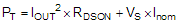
where
- PT = Total power dissipation of the device
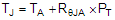
After determining the power dissipated by the device, calculate the junction temperature from the ambient temperature and the device thermal impedance.
For more information, please see the How to Drive Resistive, Inductive, Capacitive, and Lighting Loads application note.