ZHCSDJ5B January 2015 – December 2017 TPA3140D2
PRODUCTION DATA.
- 1 特性
- 2 应用
- 3 说明
- 4 修订历史记录
- 5 Device Comparison Table
- 6 Pin Configuration and Functions
- 7 Specifications
- 8 Parameter Measurement Information
-
9 Detailed Description
- 9.1 Overview
- 9.2 Functional Block Diagram
- 9.3
Feature Description
- 9.3.1 Gain Setting via GAIN Pin
- 9.3.2 SD Operation
- 9.3.3 Gain Limit Control, LIMTHRES and LIMRATE
- 9.3.4 SPEAKERGUARD Automatic Gain Limit, AGL
- 9.3.5 Thermal Foldback, TFB
- 9.3.6 PLIMIT
- 9.3.7 LIMTHRES
- 9.3.8 Spread Spectrum and De-Phase Control
- 9.3.9 GVDD Supply
- 9.3.10 DC Detect
- 9.3.11 PBTL Select
- 9.3.12 Short-Circuit Protection and Automatic Recovery Feature
- 9.3.13 Thermal Protection
- 9.4 Device Functional Modes
-
10Application and Implementation
- 10.1 Application Information
- 10.2
Typical Applications
- 10.2.1 Design Requirements
- 10.2.2
Detailed Design Procedure
- 10.2.2.1 Ferrite Bead Filter Considerations
- 10.2.2.2 Efficiency: LC Filter Required with the Traditional Class-D Modulation Scheme
- 10.2.2.3 When to Use an Output Filter for EMI Suppression
- 10.2.2.4 Input Resistance
- 10.2.2.5 Input Capacitor, Ci
- 10.2.2.6 BSN and BSP Capacitors
- 10.2.2.7 Differential Inputs
- 10.2.2.8 Using Low-ESR Capacitors
- 10.2.3 Application Performance Curves
- 11Power Supply Recommendations
- 12Layout
- 13器件和文档支持
- 14机械、封装和可订购信息
封装选项
机械数据 (封装 | 引脚)
- PWP|28
散热焊盘机械数据 (封装 | 引脚)
- PWP|28
订购信息
9.4 Device Functional Modes
The TPA3140D2 has the option of running in either BD modulation or 1SPW modulation; this is set by the 1SPW pin.
1SPW = GND: BD-modulation
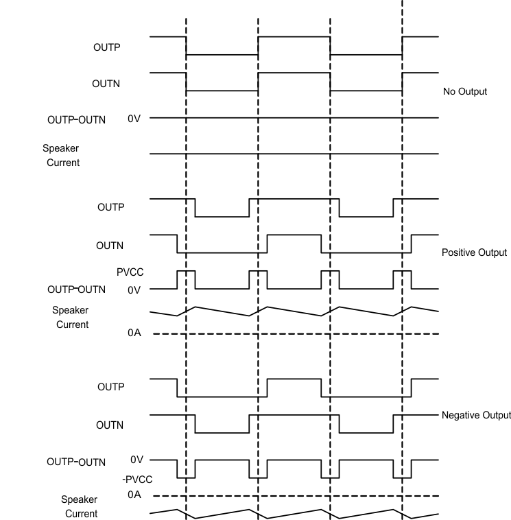
This is a modulation scheme that allows operation without the classic LC reconstruction filter when the amp is driving an inductive load with short speaker wires. Each output is switching from 0 volts to the supply voltage. The OUTPx and OUTNx are in phase with each other with no input so that there is little or no current in the speaker. The duty cycle of OUTPx is greater than 50% and OUTNx is less than 50% for positive output voltages. The duty cycle of OUTPx is less than 50% and OUTNx is greater than 50% for negative output voltages. The voltage across the load sits at 0V throughout most of the switching period, reducing the switching current, which reduces any I2R losses in the load.
 Figure 23. BD Mode Modulation
1SPW = HIGH: 1SPW-modulation
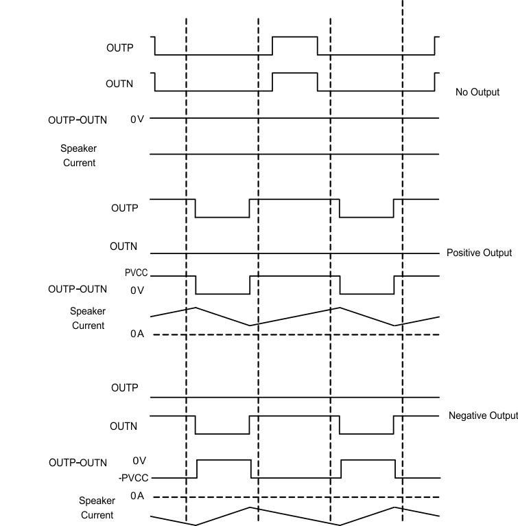
The 1SPW mode alters the normal modulation scheme in order to achieve higher efficiency with a slight penalty in THD degradation and more attention required in the output filter selection. In 1SPW mode the outputs operate at ~15% modulation during idle conditions. When an audio signal is applied one output will decrease and one will increase. The decreasing output signal will quickly rail to GND at which point all the audio modulation takes place through the rising output. The result is that only one output is switching during a majority of the audio cycle. Efficiency is improved in this mode due to the reduction of switching losses. The THD penalty in 1SPW mode is minimized by the high performance feedback loop. The resulting audio signal at each half output has a discontinuity each time the output rails to GND. This can cause ringing in the audio reconstruction filter unless care is taken in the selection of the filter components and type of filter used.
 Figure 24. 1SPW Mode Modulation