ZHCSDJ5B January 2015 – December 2017 TPA3140D2
PRODUCTION DATA.
- 1 特性
- 2 应用
- 3 说明
- 4 修订历史记录
- 5 Device Comparison Table
- 6 Pin Configuration and Functions
- 7 Specifications
- 8 Parameter Measurement Information
-
9 Detailed Description
- 9.1 Overview
- 9.2 Functional Block Diagram
- 9.3
Feature Description
- 9.3.1 Gain Setting via GAIN Pin
- 9.3.2 SD Operation
- 9.3.3 Gain Limit Control, LIMTHRES and LIMRATE
- 9.3.4 SPEAKERGUARD Automatic Gain Limit, AGL
- 9.3.5 Thermal Foldback, TFB
- 9.3.6 PLIMIT
- 9.3.7 LIMTHRES
- 9.3.8 Spread Spectrum and De-Phase Control
- 9.3.9 GVDD Supply
- 9.3.10 DC Detect
- 9.3.11 PBTL Select
- 9.3.12 Short-Circuit Protection and Automatic Recovery Feature
- 9.3.13 Thermal Protection
- 9.4 Device Functional Modes
-
10Application and Implementation
- 10.1 Application Information
- 10.2
Typical Applications
- 10.2.1 Design Requirements
- 10.2.2
Detailed Design Procedure
- 10.2.2.1 Ferrite Bead Filter Considerations
- 10.2.2.2 Efficiency: LC Filter Required with the Traditional Class-D Modulation Scheme
- 10.2.2.3 When to Use an Output Filter for EMI Suppression
- 10.2.2.4 Input Resistance
- 10.2.2.5 Input Capacitor, Ci
- 10.2.2.6 BSN and BSP Capacitors
- 10.2.2.7 Differential Inputs
- 10.2.2.8 Using Low-ESR Capacitors
- 10.2.3 Application Performance Curves
- 11Power Supply Recommendations
- 12Layout
- 13器件和文档支持
- 14机械、封装和可订购信息
封装选项
机械数据 (封装 | 引脚)
- PWP|28
散热焊盘机械数据 (封装 | 引脚)
- PWP|28
订购信息
9.3.4 SPEAKERGUARD Automatic Gain Limit, AGL
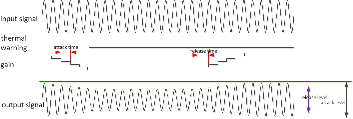
The TPA3140D2 has a built-in SpeakerGuard AGL to limit excessive output voltage to a non clipping output signal. When an excessive level input signal is sent to TPA3140D2, the SpeakerGuard AGL will automatically reduce the amplifier gain to maintain maximum unclipped output signal to preserve high audio quality and to protect the attached speaker from excessive power. The AGL works with a fast attack speed and a slower release speed to achieve maximum protection and a minimum number of audible artifacts.
 Figure 17. AGL Attack and Release Thresholds
When the input level multiplied by the TPA3140D2 closed loop gain exceeds the limiter threshold set by the LIMTHRES pin voltage, the TPA3140D2 closed loop gain is reduced by a single or by multiple 0.5-dB steps until the output signal voltage gets below the level set by the LIMTHRES pin voltage, or if a –12.0-dB gain reduction limit is reached. When the output voltage gets below the release threshold, the TPA3140D2 closed loop gain is increased by a single or by multiple 0.5-dB steps until the release threshold is reached, or the closed loop gain is at its nominal closed loop gain level. The AGL gain adjustment is applied with a ramp speed selectable by the LIMRATE pin setting.
 Figure 18. AGL Attack and Release Slopes