ZHCSDJ5B January 2015 – December 2017 TPA3140D2
PRODUCTION DATA.
- 1 特性
- 2 应用
- 3 说明
- 4 修订历史记录
- 5 Device Comparison Table
- 6 Pin Configuration and Functions
- 7 Specifications
- 8 Parameter Measurement Information
-
9 Detailed Description
- 9.1 Overview
- 9.2 Functional Block Diagram
- 9.3
Feature Description
- 9.3.1 Gain Setting via GAIN Pin
- 9.3.2 SD Operation
- 9.3.3 Gain Limit Control, LIMTHRES and LIMRATE
- 9.3.4 SPEAKERGUARD Automatic Gain Limit, AGL
- 9.3.5 Thermal Foldback, TFB
- 9.3.6 PLIMIT
- 9.3.7 LIMTHRES
- 9.3.8 Spread Spectrum and De-Phase Control
- 9.3.9 GVDD Supply
- 9.3.10 DC Detect
- 9.3.11 PBTL Select
- 9.3.12 Short-Circuit Protection and Automatic Recovery Feature
- 9.3.13 Thermal Protection
- 9.4 Device Functional Modes
-
10Application and Implementation
- 10.1 Application Information
- 10.2
Typical Applications
- 10.2.1 Design Requirements
- 10.2.2
Detailed Design Procedure
- 10.2.2.1 Ferrite Bead Filter Considerations
- 10.2.2.2 Efficiency: LC Filter Required with the Traditional Class-D Modulation Scheme
- 10.2.2.3 When to Use an Output Filter for EMI Suppression
- 10.2.2.4 Input Resistance
- 10.2.2.5 Input Capacitor, Ci
- 10.2.2.6 BSN and BSP Capacitors
- 10.2.2.7 Differential Inputs
- 10.2.2.8 Using Low-ESR Capacitors
- 10.2.3 Application Performance Curves
- 11Power Supply Recommendations
- 12Layout
- 13器件和文档支持
- 14机械、封装和可订购信息
封装选项
机械数据 (封装 | 引脚)
- PWP|28
散热焊盘机械数据 (封装 | 引脚)
- PWP|28
订购信息
9.3.1 Gain Setting via GAIN Pin
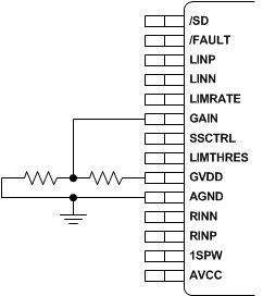
The gain of the TPA3140D2 is set by a voltage applied to the GAIN pin, which is set by a resistor voltage divider with GVDD as supply voltage. The resistance of the voltage divider should be a minimum of 100 kΩ in order not to overload the GVDD regulator of TPA3140D2.
 Figure 16. GAIN Pin Voltage Programming by GVDD Resistor Divider
The gains listed in Table 1 are realized by changing the taps on the input resistors and feedback resistors inside the amplifier. This causes the input impedance (Zi) to be dependent on the gain setting. The actual gain settings are controlled by ratios of resistors, so the gain variation from part-to-part is small. However, the input impedance from part-to-part at the same gain may shift by ±20% due to shifts in the actual resistance of the input resistors. The selected input gain is latched at device start up and cannot be changed when SD is high.
For design purposes, the input network (discussed in the next section) should be designed assuming an input impedance of 7.2 kΩ, which is the absolute minimum input impedance of the TPA3140D2. At the lower gain settings, the input impedance could increase as high as 72 kΩ.
Table 1. Gain Setting
| GAIN PIN VOLTAGE | AMPLIFIER GAIN (dB) | INPUT IMPEDANCE (kΩ) |
| TYP | TYP | |
| 0 V (GND) | 20 | 60 |
| 2.3 V (1/3·GVDD) | 26 | 30 |
| 4.6 V (2/3·GVDD) | 32 | 15 |
| 6.9 V (GVDD) | 36 | 9 |