ZHCSAA3B September 2012 – September 2015 TPA3112D1-Q1
PRODUCTION DATA.
- 1 特性
- 2 应用
- 3 说明
- 4 修订历史记录
- 5 Pin Configuration and Functions
- 6 Specifications
- 7 Detailed Description
-
8 Application and Implementation
- 8.1 Application Information
- 8.2
Typical Application
- 8.2.1 Design Requirements
- 8.2.2
Detailed Design Procedure
- 8.2.2.1 Class-D Operation
- 8.2.2.2 TPA3112D1-Q1 Modulation Scheme
- 8.2.2.3 Ferrite Bead Filter Considerations
- 8.2.2.4 Efficiency: LC Filter Required With the Traditional Class-D Modulation Scheme
- 8.2.2.5 When to Use an Output Filter for EMI Suppression
- 8.2.2.6 Input Resistance
- 8.2.2.7 Input Capacitor, CI
- 8.2.2.8 BSN and BSP Capacitors
- 8.2.2.9 Differential Inputs
- 8.2.2.10 Using Low-ESR Capacitors
- 8.2.3 Application Curves
- 9 Power Supply Recommendations
- 10Layout
- 11器件和文档支持
- 12机械、封装和可订购信息
6 Specifications
6.1 Absolute Maximum Ratings
over operating free-air temperature range (unless otherwise noted)(1)| MIN | MAX | UNIT | |||
|---|---|---|---|---|---|
| VCC | Supply voltage | AVCC, PVCC | –0.3 | 30 | V |
| VI | Interface pin voltage | SD, FAULT,GAIN0, GAIN1, AVCC (Pin 14) (2) | –0.3 | VCC + 0.3 | V |
| < 10 | V/ms | ||||
| PLIMIT | –0.3 | GVDD + 0.3 | V | ||
| INN, INP | –0.3 | 6.3 | V | ||
| RL | Minimum Load Resistance | BTL | 3.2 | ||
| Continuous total power dissipation | See Thermal Information Table | ||||
| TA | Operating free-air temperature range | –40 | 125 | °C | |
| TJ | Operating junction temperature range(3) | –40 | 150 | °C | |
| Tstg | Storage temperature range | –65 | 150 | °C | |
(1) Stresses beyond those listed under absolute maximum ratings may cause permanent damage to the device. These are stress ratings only, and functional operations of the device at these or any other conditions beyond those indicated under recommended operating conditions is not implied. Exposure to absolute-maximum-rated conditions for extended periods may affect device reliability.
(2) The voltage slew rate of these pins must be restricted to no more than 10 V/ms. For higher slew rates, use a 100 kΩ resister in series with the pins, per application note SLUA626.
(3) The TPA3112D1-Q1 incorporates an exposed thermal pad on the underside of the chip. This acts as a heatsink, and it must be connected to a thermally dissipating plane for proper power dissipation. Failure to do so may result in the device going into thermal protection shutdown. See TI Technical Briefs SCBA017 and SLUA271 for more information about using the QFN thermal pad. See TI Technical Brief SLMA002 for more information about using the HTQFP thermal pad.
6.2 ESD Ratings
| VALUE | UNIT | |||
|---|---|---|---|---|
| V(ESD) | Electrostatic discharge | Human-body model (HBM), per AEC Q100-002(1) | ±4000 | V |
| Charged-device model (CDM), per AEC Q100-011 | ±250 | |||
| Machine model (MM) per JESD22-A115 | ±200 | |||
(1) AEC Q100-002 indicates that HBM stressing shall be in accordance with the ANSI/ESDA/JEDEC JS-001 specification.
6.3 Recommended Operating Conditions
over operating free-air temperature range (unless otherwise noted)| MIN | MAX | UNIT | |||
|---|---|---|---|---|---|
| VCC | Supply voltage | PVCC, AVCC | 8 | 26 | V |
| VIH | High-level input voltage | SD, GAIN0, GAIN1 | 2 | V | |
| VIL | Low-level input voltage | SD, GAIN0, GAIN1 | 0.8 | V | |
| VOL | Low-level output voltage | FAULT, RPULLUP = 100 kΩ, VCC = 26 V | 0.8 | V | |
| IIH | High-level input current | SD, GAIN0, GAIN1, VI = 2, VCC = 18 V | 50 | µA | |
| IIL | Low-level input current | SD, GAIN0, GAIN1, VI = 0.8 V, VCC = 18 V | 5 | µA | |
| TA | Operating free-air temperature | –40 | 125 | °C | |
6.4 Thermal Information
| THERMAL METRIC(1)(2) | TPA3112D1-Q1 | UNIT | |
|---|---|---|---|
| PWP (HTSSOP) | |||
| 28 PINS | |||
| RθJA | Junction-to-ambient thermal resistance | 30.3 | °C/W |
| RθJC(top) | Junction-to-case (top) thermal resistance | 33.5 | °C/W |
| RθJB | Junction-to-board thermal resistance | 17.5 | °C/W |
| ψJT | Junction-to-top characterization parameter | 0.9 | °C/W |
| ψJB | Junction-to-board characterization parameter | 7.2 | °C/W |
| RθJC(bot) | Junction-to-case (bottom) thermal resistance | 0.9 | °C/W |
(1) For more information about traditional and new thermal metrics, see the Semiconductor and IC Package Thermal Metrics application report, SPRA953.
(2) For thermal estimates of this device based on PCB copper area, see the TI PCB Thermal Calculator
6.5 DC Characteristics
TA = –40°C to 125°C, VCC = 24 V, RL = 8 Ω (unless otherwise noted)6.6 DC Characteristics
TA = –40°C to 125°C, VCC = 12 V, RL = 8 Ω (unless otherwise noted)| PARAMETER | TEST CONDITIONS | MIN | TYP | MAX | UNIT | ||
|---|---|---|---|---|---|---|---|
| | VOS | | Class-D output offset voltage (measured differentially) | VI = 0 V, Gain = 36 dB | 1.5 | 15 | mV | ||
| ICC | Quiescent supply current | SD = 2 V, no load, PVCC = 12 V | 20 | mA | |||
| ICC(SD) | Quiescent supply current in shutdown mode | SD = 0.8 V, no load, PVCC = 12 V | 200 | µA | |||
| rDS(on) | Drain-source on-state resistance | IO = 500 mA, TJ = 25°C |
High side | 240 | mΩ | ||
| Low side | 240 | ||||||
| G | Gain | GAIN1 = 0.8 V | GAIN0 = 0.8 V | 19 | 20 | 21 | dB |
| GAIN0 = 2 V | 25 | 26 | 27 | ||||
| GAIN1 = 2 V | GAIN0 = 0.8 V | 31 | 32 | 33 | dB | ||
| GAIN0 = 2 V | 35 | 36 | 37 | ||||
| tON | Turn-on time | SD = 2 V | 10 | ms | |||
| tOFF | Turn-off time | SD = 0.8 V | 2 | μs | |||
| GVDD | Gate Drive Supply | IGVDD = 2 mA | 6.5 | 6.9 | 7.3 | V | |
| PLIMIT | Output Voltage maximum under PLIMIT control | VPLIMIT = 2.0 V; VI = 6-V differential | 6.75 | 7.90 | 8.75 | V | |
6.7 AC Characteristics
TA = –40°C to 125°C, VCC = 24 V, RL = 8 Ω (unless otherwise noted)| PARAMETER | TEST CONDITIONS | MIN | TYP | MAX | UNIT | |
|---|---|---|---|---|---|---|
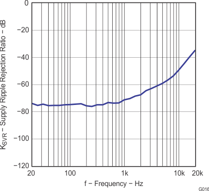
| KSVR | Power Supply ripple rejection | 200 mVPP ripple from 20 Hz–1 kHz, Gain = 20 dB, inputs AC-coupled to AGND |
–70 | dB | ||
| PO | Continuous output power | THD+N ≤ 0.1%, f = 1 kHz, VCC = 24 V | 25 | W | ||
| THD+N | Total harmonic distortion + noise | VCC = 24 V, f = 1 kHz, PO = 12 W (half-power) | <0.05 % | |||
| Vn | Output integrated noise | 20 Hz to 22 kHz, A-weighted filter, Gain = 20 dB | 65 | µV | ||
| –80 | dBV | |||||
| Crosstalk | VO = 1 Vrms, Gain = 20 dB, f = 1 kHz | –70 | dB | |||
| SNR | Signal-to-noise ratio | Maximum output at THD+N < 1%, f = 1 kHz, Gain = 20 dB, A-weighted |
102 | dB | ||
| fOSC | Oscillator frequency | 250 | 310 | 350 | kHz | |
| Thermal trip point | 150 | °C | ||||
| Thermal hysteresis | 15 | °C | ||||
6.8 AC Characteristics
TA = –40°C to 125°C, VCC = 12 V, RL = 8 Ω (unless otherwise noted)| PARAMETER | TEST CONDITIONS | MIN | TYP | MAX | UNIT | |
|---|---|---|---|---|---|---|
| KSVR | Supply ripple rejection | 200 mVPP ripple from 20 Hz–1 kHz, Gain = 20 dB, inputs AC-coupled to AGND |
–70 | dB | ||
| PO | Continuous output power | THD+N ≤ 10%, f = 1 kHz , RL = 8 Ω | 10 | W | ||
| PO | Continuous output power | THD+N ≤ 10%, f = 1 kHz , RL = 4 Ω | 20 | W | ||
| THD+N | Total harmonic distortion + noise | RL = 8 Ω, f = 1 kHz, PO = 5 W (half-power) | <0.06 % | |||
| Vn | Output integrated noise | 20 Hz to 22 kHz, A-weighted filter, Gain = 20 dB | 65 | µV | ||
| –80 | dBV | |||||
| Crosstalk | Po = 1 W, Gain = 20 dB, f = 1 kHz | –70 | dB | |||
| SNR | Signal-to-noise ratio | Maximum output at THD+N < 1%, f = 1 kHz, Gain = 20 dB, A-weighted |
102 | dB | ||
| fOSC | Oscillator frequency | 250 | 310 | 350 | kHz | |
| Thermal trip point | 150 | °C | ||||
| Thermal hysteresis | 15 | °C | ||||
6.9 Typical Characteristics
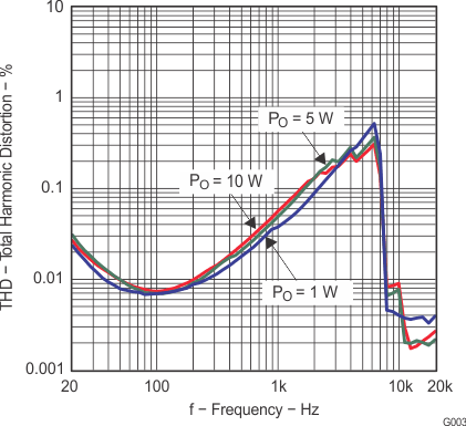
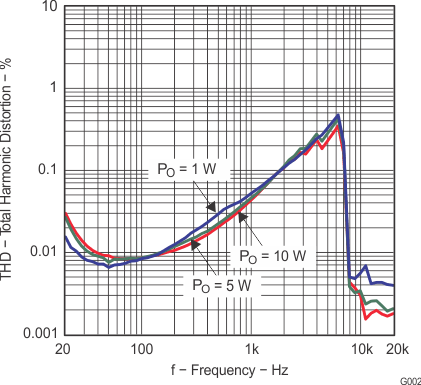
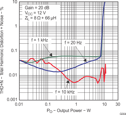
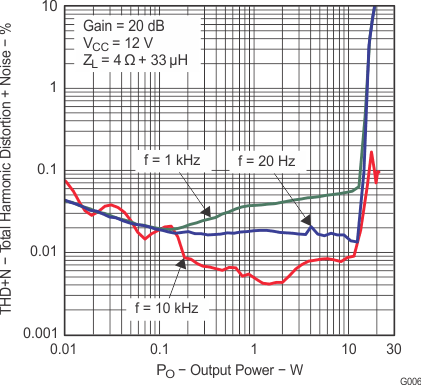
All measurements taken at 1 kHz, unless otherwise noted. The TPA3112D2 EVM (which is available at ti.com) made these measurements.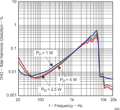
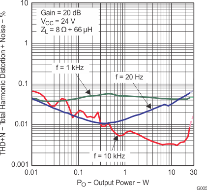
Note: Lighter colored lines represent thermally limited region.
Figure 5. Total Harmonic Distortion + Noise vs Output Power
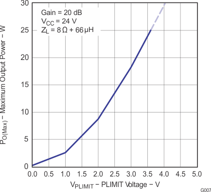
Note: Lighter color represents thermally limited region.
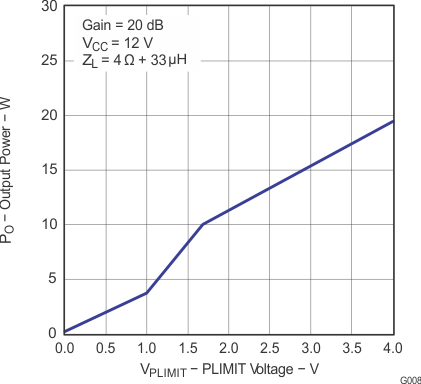
Figure 7. Maximum Output Power vs Plimit Voltage
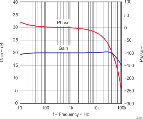
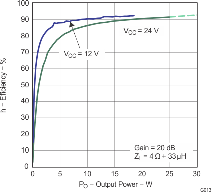
Note: Lighter color represents thermally limited region.
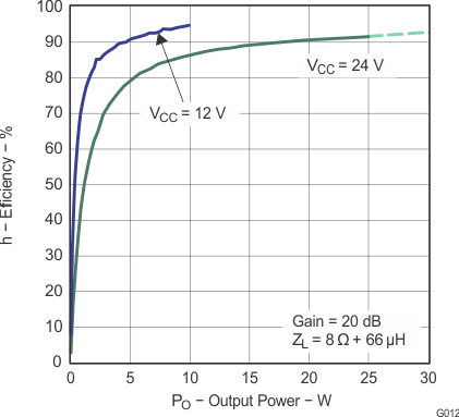
Figure 11. Efficiency vs Output Power
Note: Lighter color represents thermally limited region.
Figure 10. Efficiency vs Output Power
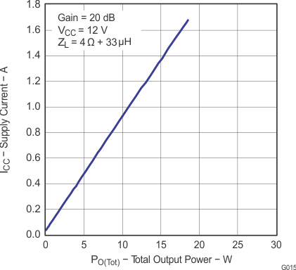
Note: Lighter color represents thermally limited region.
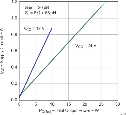
Figure 12. Supply Current vs Total Output Power
