ZHCSAA3B September 2012 – September 2015 TPA3112D1-Q1
PRODUCTION DATA.
- 1 特性
- 2 应用
- 3 说明
- 4 修订历史记录
- 5 Pin Configuration and Functions
- 6 Specifications
- 7 Detailed Description
-
8 Application and Implementation
- 8.1 Application Information
- 8.2
Typical Application
- 8.2.1 Design Requirements
- 8.2.2
Detailed Design Procedure
- 8.2.2.1 Class-D Operation
- 8.2.2.2 TPA3112D1-Q1 Modulation Scheme
- 8.2.2.3 Ferrite Bead Filter Considerations
- 8.2.2.4 Efficiency: LC Filter Required With the Traditional Class-D Modulation Scheme
- 8.2.2.5 When to Use an Output Filter for EMI Suppression
- 8.2.2.6 Input Resistance
- 8.2.2.7 Input Capacitor, CI
- 8.2.2.8 BSN and BSP Capacitors
- 8.2.2.9 Differential Inputs
- 8.2.2.10 Using Low-ESR Capacitors
- 8.2.3 Application Curves
- 9 Power Supply Recommendations
- 10Layout
- 11器件和文档支持
- 12机械、封装和可订购信息
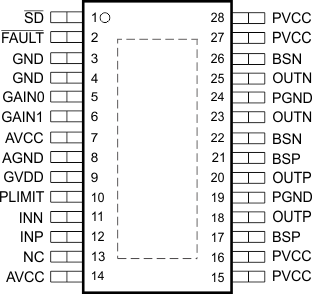
5 Pin Configuration and Functions
PWP Package
28-Pin HTSSOP With PowerPAD™ IC
Top View

Pin Functions
| PIN | TYPE | DESCRIPTION | |
|---|---|---|---|
| NO. | NAME | ||
| 1 | SD | I | Shutdown logic input for audio amp (LOW = outputs Hi-Z, HIGH = outputs enabled). TTL logic levels with compliance to AVCC. |
| 2 | FAULT | O | Open drain output used to display short circuit or DC detect fault status. Voltage compliant to AVCC. Short circuit faults can be set to auto-recovery by connecting FAULT pin to SD pin. Otherwise both the short circuit faults and DC detect faults must be reset by cycling PVCC. |
| 3 | GND | — | Connect to local ground. |
| 4 | GND | — | Connect to local ground. |
| 5 | GAIN0 | I | Gain select least significant bit. TTL logic levels with compliance to AVCC. |
| 6 | GAIN1 | I | Gain select most significant bit. TTL logic levels with compliance to AVCC. |
| 7 | AVCC | P | Analog supply |
| 8 | AGND | — | Analog supply ground. Connect to the thermal pad. |
| 9 | GVDD | O | High-side FET gate drive supply. Nominal voltage is 7 V. May also be used as supply for PLIMIT divider. Add a 1-μF cap to ground at this pin. |
| 10 | PLIMIT | I | Power limit level adjust. Connect directly to GVDD pin for no power limiting. Add a 1-μF cap to ground at this pin. |
| 11 | INN | I | Negative audio input. Biased at 3 V. |
| 12 | INP | I | Positive audio input. Biased at 3 V. |
| 13 | NC | — | Not connected |
| 14 | AVCC | P | Connect AVCC supply to this pin. |
| 15 | PVCC | P | Power supply for H-bridge. PVCC pins are also connected internally. |
| 16 | PVCC | P | Power supply for H-bridge. PVCC pins are also connected internally. |
| 17 | BSP | I | Bootstrap I/O for positive high-side FET. |
| 18 | OUTP | O | Class-D H-bridge positive output. |
| 19 | PGND | — | Power ground for the H-bridges. |
| 20 | OUTP | O | Class-D H-bridge positive output. |
| 21 | BSP | I | Bootstrap I/O for positive high-side FET. |
| 22 | BSN | I | Bootstrap I/O for negative high-side FET. |
| 23 | OUTN | O | Class-D H-bridge negative output. |
| 24 | PGND | — | Power ground for the H-bridges. |
| 25 | OUTN | O | Class-D H-bridge negative output. |
| 26 | BSN | I | Bootstrap I/O for negative high-side FET. |
| 27 | PVCC | P | Power supply for H-bridge. PVCC pins are also connected internally. |
| 28 | PVCC | P | Power supply for H-bridge. PVCC pins are also connected internally. |