ZHCSE08D May   2015  – January 2020 TMP107

PRODUCTION DATA.  

  1. 特性
  2. 应用范围
  3. 说明
    1.     Device Images
      1.      典型应用
  4. 修订历史记录
  5. Pin Configuration and Functions
    1.     Pin Functions
  6. Specifications
    1. 6.1 Absolute Maximum Ratings
    2. 6.2 ESD Ratings
    3. 6.3 Recommended Operating Conditions
    4. 6.4 Thermal Information
    5. 6.5 Electrical Characteristics
    6. 6.6 Timing Requirements
    7. 6.7 Typical Characteristics
  7. Detailed Description
    1. 7.1 Overview
    2. 7.2 Functional Block Diagram
    3. 7.3 Feature Description
      1. 7.3.1 Digital Temperature Output
      2. 7.3.2 Temperature Limits and Alert
        1. 7.3.2.1 ALERT1, ALERT2, R1, and R2 Pins
      3. 7.3.3 SMAART Wire™ Communication Interface
        1. 7.3.3.1 Communication Protocol
          1. 7.3.3.1.1 Calibration Phase
          2. 7.3.3.1.2 Command and Address Phase
            1. 7.3.3.1.2.1 Global or Individual (G/nI) Bit
            2. 7.3.3.1.2.2 Read/Write (R/nW) Bit
            3. 7.3.3.1.2.3 Command or Address (C/nA) Bit:
          3. 7.3.3.1.3 Register Pointer Phase
          4. 7.3.3.1.4 Data Phase
        2. 7.3.3.2 SMAART Wire™ Operations
          1. 7.3.3.2.1 Command Operations
            1. 7.3.3.2.1.1 Address Initialize
            2. 7.3.3.2.1.2 Last Device Poll
            3. 7.3.3.2.1.3 Global Software Reset
          2. 7.3.3.2.2 Address Operations
            1. 7.3.3.2.2.1 Individual Write
            2. 7.3.3.2.2.2 Individual Read
            3. 7.3.3.2.2.3 Global Write
            4. 7.3.3.2.2.4 Global Read
    4. 7.4 Device Functional Modes
      1. 7.4.1 Continuous-Conversion Mode
      2. 7.4.2 Shutdown Mode
      3. 7.4.3 One-Shot Mode
    5. 7.5 Programming
      1. 7.5.1 EEPROM
      2. 7.5.2 EEPROM Operations
        1. 7.5.2.1 EEPROM Unlock
        2. 7.5.2.2 EEPROM Lock
        3. 7.5.2.3 EEPROM Programming
        4. 7.5.2.4 EEPROM Acquire or Read
    6. 7.6 Register Map
      1. 7.6.1 Temperature Register (address = 0h) [reset = 0h]
        1. Table 4. Temperature Register Field Descriptions
      2. 7.6.2 Configuration Register (address = 1h) [reset = A000h]
        1. Table 5. Configuration Register Field Descriptions
      3. 7.6.3 High Limit 1 Register (address = 2h) [reset = 7FFCh]
        1. Table 7. High Limit 1 Register Field Descriptions
      4. 7.6.4 Low Limit 1 Register (address = 3h) [reset = 8000h]
        1. Table 8. Low Limit 1 Register Field Descriptions
      5. 7.6.5 High Limit 2 Register (address = 4h) [reset = 7FFCh]
        1. Table 9. High Limit 2 Register Field Descriptions
      6. 7.6.6 Low Limit 2 Register (address = 5h) [reset = 8000h]
        1. Table 10. Low Limit 2 Register Field Descriptions
      7. 7.6.7 EEPROM n Register (where n = 1 to 8) (addresses = 6h to Dh) [reset = 0h]
        1. Table 11. EEPROM Register bits
      8. 7.6.8 Die ID Register (address = Fh) [reset = 1107h]
        1. Table 12. Die ID Register Field Descriptions
  8. Application and Implementation
    1. 8.1 Application Information
    2. 8.2 Typical Applications
      1. 8.2.1 Connecting Multiple Devices
        1. 8.2.1.1 Design Requirements
        2. 8.2.1.2 Detailed Design Procedure
          1. 8.2.1.2.1 Voltage Drop Effect
          2. 8.2.1.2.2 EEPROM Programming Current
          3. 8.2.1.2.3 Power Savings
          4. 8.2.1.2.4 Accuracy
          5. 8.2.1.2.5 Electromagnetic Interference (EMI)
        3. 8.2.1.3 Application Curves
      2. 8.2.2 Connecting ALERT1 and ALERT2 Pins
      3. 8.2.3 ALERT1 and ALERT2 Pins Used as General-Purpose Output (GPO)
  9. Power Supply Recommendations
  10. 10Layout
    1. 10.1 Layout Guidelines
    2. 10.2 Layout Example
  11. 11器件和文档支持
    1. 11.1 文档支持
      1. 11.1.1 相关文档
    2. 11.2 接收文档更新通知
    3. 11.3 社区资源
    4. 11.4 商标
    5. 11.5 静电放电警告
    6. 11.6 Glossary
  12. 12机械、封装和可订购信息

封装选项

机械数据 (封装 | 引脚)
散热焊盘机械数据 (封装 | 引脚)
订购信息

Application Curves

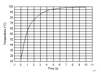
Figure 40 shows the step response of the TMP107 to a submersion in an oil bath of 100ºC from room temperature (24ºC) at a 3.3-V supply. The time-constant, or the time for the output to reach 63% of the input step, is 1.375 s. The time-constant depends on the printed-circuit board (PCB) that the device is mounted on. For this test, the device is soldered to a two-layer PCB that measures 0.551 in × 0.748 in.

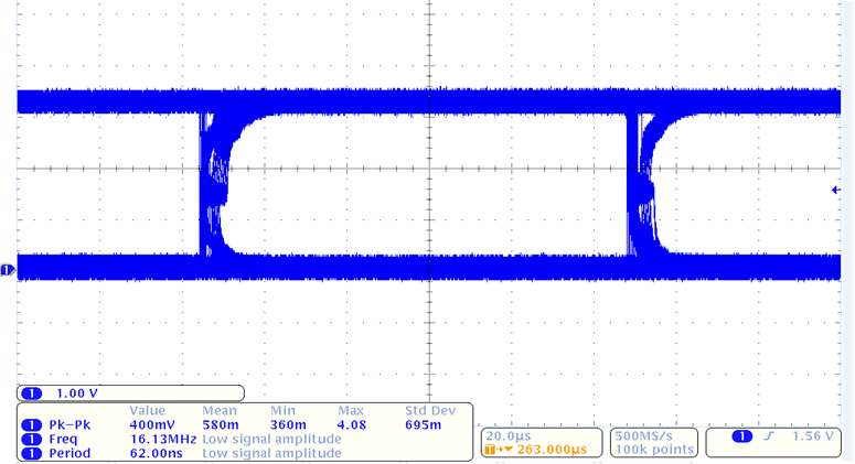
Figure 41 shows the TMP107 eye diagram as a measure of quality for the transmission path (cable). Measurement of eye patterns is performed by a setup where a source generates a known bit stream that is fed into a transmission channel. The eye diagram of TMP107 is taken on the I/O line at the far end of a 300-meter cable connecting two TMP107 devices. The baud rate is 9600 bps, and the supply voltage is set to 3.3 V. The scope is set to trigger on I/O rising (or falling) edge, with an infinite persistent time. The superimposed, captured waveforms create the eye diagram. Excellent eye diagram parameters are maintained at 9600 bps speed.
TMP107 D001_TMP107B.gif
Figure 40. Temperature Step Response
TMP107 eyediagram_sbos716.gif
Figure 41. TMP107 Eye Diagram