ZHCSE08D May   2015  – January 2020 TMP107

PRODUCTION DATA.  

  1. 特性
  2. 应用范围
  3. 说明
    1.     Device Images
      1.      典型应用
  4. 修订历史记录
  5. Pin Configuration and Functions
    1.     Pin Functions
  6. Specifications
    1. 6.1 Absolute Maximum Ratings
    2. 6.2 ESD Ratings
    3. 6.3 Recommended Operating Conditions
    4. 6.4 Thermal Information
    5. 6.5 Electrical Characteristics
    6. 6.6 Timing Requirements
    7. 6.7 Typical Characteristics
  7. Detailed Description
    1. 7.1 Overview
    2. 7.2 Functional Block Diagram
    3. 7.3 Feature Description
      1. 7.3.1 Digital Temperature Output
      2. 7.3.2 Temperature Limits and Alert
        1. 7.3.2.1 ALERT1, ALERT2, R1, and R2 Pins
      3. 7.3.3 SMAART Wire™ Communication Interface
        1. 7.3.3.1 Communication Protocol
          1. 7.3.3.1.1 Calibration Phase
          2. 7.3.3.1.2 Command and Address Phase
            1. 7.3.3.1.2.1 Global or Individual (G/nI) Bit
            2. 7.3.3.1.2.2 Read/Write (R/nW) Bit
            3. 7.3.3.1.2.3 Command or Address (C/nA) Bit:
          3. 7.3.3.1.3 Register Pointer Phase
          4. 7.3.3.1.4 Data Phase
        2. 7.3.3.2 SMAART Wire™ Operations
          1. 7.3.3.2.1 Command Operations
            1. 7.3.3.2.1.1 Address Initialize
            2. 7.3.3.2.1.2 Last Device Poll
            3. 7.3.3.2.1.3 Global Software Reset
          2. 7.3.3.2.2 Address Operations
            1. 7.3.3.2.2.1 Individual Write
            2. 7.3.3.2.2.2 Individual Read
            3. 7.3.3.2.2.3 Global Write
            4. 7.3.3.2.2.4 Global Read
    4. 7.4 Device Functional Modes
      1. 7.4.1 Continuous-Conversion Mode
      2. 7.4.2 Shutdown Mode
      3. 7.4.3 One-Shot Mode
    5. 7.5 Programming
      1. 7.5.1 EEPROM
      2. 7.5.2 EEPROM Operations
        1. 7.5.2.1 EEPROM Unlock
        2. 7.5.2.2 EEPROM Lock
        3. 7.5.2.3 EEPROM Programming
        4. 7.5.2.4 EEPROM Acquire or Read
    6. 7.6 Register Map
      1. 7.6.1 Temperature Register (address = 0h) [reset = 0h]
        1. Table 4. Temperature Register Field Descriptions
      2. 7.6.2 Configuration Register (address = 1h) [reset = A000h]
        1. Table 5. Configuration Register Field Descriptions
      3. 7.6.3 High Limit 1 Register (address = 2h) [reset = 7FFCh]
        1. Table 7. High Limit 1 Register Field Descriptions
      4. 7.6.4 Low Limit 1 Register (address = 3h) [reset = 8000h]
        1. Table 8. Low Limit 1 Register Field Descriptions
      5. 7.6.5 High Limit 2 Register (address = 4h) [reset = 7FFCh]
        1. Table 9. High Limit 2 Register Field Descriptions
      6. 7.6.6 Low Limit 2 Register (address = 5h) [reset = 8000h]
        1. Table 10. Low Limit 2 Register Field Descriptions
      7. 7.6.7 EEPROM n Register (where n = 1 to 8) (addresses = 6h to Dh) [reset = 0h]
        1. Table 11. EEPROM Register bits
      8. 7.6.8 Die ID Register (address = Fh) [reset = 1107h]
        1. Table 12. Die ID Register Field Descriptions
  8. Application and Implementation
    1. 8.1 Application Information
    2. 8.2 Typical Applications
      1. 8.2.1 Connecting Multiple Devices
        1. 8.2.1.1 Design Requirements
        2. 8.2.1.2 Detailed Design Procedure
          1. 8.2.1.2.1 Voltage Drop Effect
          2. 8.2.1.2.2 EEPROM Programming Current
          3. 8.2.1.2.3 Power Savings
          4. 8.2.1.2.4 Accuracy
          5. 8.2.1.2.5 Electromagnetic Interference (EMI)
        3. 8.2.1.3 Application Curves
      2. 8.2.2 Connecting ALERT1 and ALERT2 Pins
      3. 8.2.3 ALERT1 and ALERT2 Pins Used as General-Purpose Output (GPO)
  9. Power Supply Recommendations
  10. 10Layout
    1. 10.1 Layout Guidelines
    2. 10.2 Layout Example
  11. 11器件和文档支持
    1. 11.1 文档支持
      1. 11.1.1 相关文档
    2. 11.2 接收文档更新通知
    3. 11.3 社区资源
    4. 11.4 商标
    5. 11.5 静电放电警告
    6. 11.6 Glossary
  12. 12机械、封装和可订购信息

封装选项

机械数据 (封装 | 引脚)
散热焊盘机械数据 (封装 | 引脚)
订购信息

Global Read

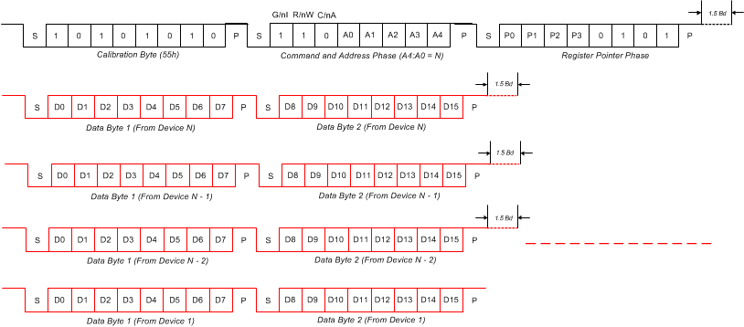
Use the global read address operation to read the value of the register pointed to by the Register Pointer Phase section. The daisy chain returns data starting from the address specified in the command or address phase, and ending with the address of the first device in the daisy chain. The data phase of the global read address operation is different from other address operations because the data phase consists of data read back from every device on the bus between the addressed device and first device, as shown in Figure 29. If the address specified exceeds the address of the last device, the operation halts and the bus times out after 35 ms. There is a delay of up to 1.5 baud before the devices respond back to the host. The host reads the data from the devices by synchronizing to the falling edge of the start bits.
TMP107 global_read_sbos716.gifFigure 29. Global Read Operation