ZHCSE08D May 2015 – January 2020 TMP107
PRODUCTION DATA.
- 1 特性
- 2 应用范围
- 3 说明
- 4 修订历史记录
- 5 Pin Configuration and Functions
- 6 Specifications
-
7 Detailed Description
- 7.1 Overview
- 7.2 Functional Block Diagram
- 7.3 Feature Description
- 7.4 Device Functional Modes
- 7.5 Programming
- 7.6
Register Map
- 7.6.1 Temperature Register (address = 0h) [reset = 0h]
- 7.6.2 Configuration Register (address = 1h) [reset = A000h]
- 7.6.3 High Limit 1 Register (address = 2h) [reset = 7FFCh]
- 7.6.4 Low Limit 1 Register (address = 3h) [reset = 8000h]
- 7.6.5 High Limit 2 Register (address = 4h) [reset = 7FFCh]
- 7.6.6 Low Limit 2 Register (address = 5h) [reset = 8000h]
- 7.6.7 EEPROM n Register (where n = 1 to 8) (addresses = 6h to Dh) [reset = 0h]
- 7.6.8 Die ID Register (address = Fh) [reset = 1107h]
- 8 Application and Implementation
- 9 Power Supply Recommendations
- 10Layout
- 11器件和文档支持
- 12机械、封装和可订购信息
7.3.2 Temperature Limits and Alert
The TMP107 has two ALERTx pins (ALERT1 and ALERT2) for under- and overtemperature monitor functions. Both pins have independent, dynamically-programmable limits. At the end of each conversion, the temperature result is compared with the high limit and low limit registers. If the temperature is outside the limit window, the respective ALERTx pin trips. There are two polarity bits that set the active state of the ALERTx pin. The TMP107 has two flag bits (FHx and FLx) for each alert condition to indicate in which direction the temperature has moved outside of the limit window.
There are two operating modes used for alerts and flags: therm and alert. In therm mode, the ALERTx pins and FHx and FLx flags are outputs of a transparent comparator. In alert mode, the ALERTx pins and FHx and FLx flags are latched interrupts. Select between alert mode or therm mode by using the Tx/Ax (T1/A1 and T2/A2) bits in the configuration register.
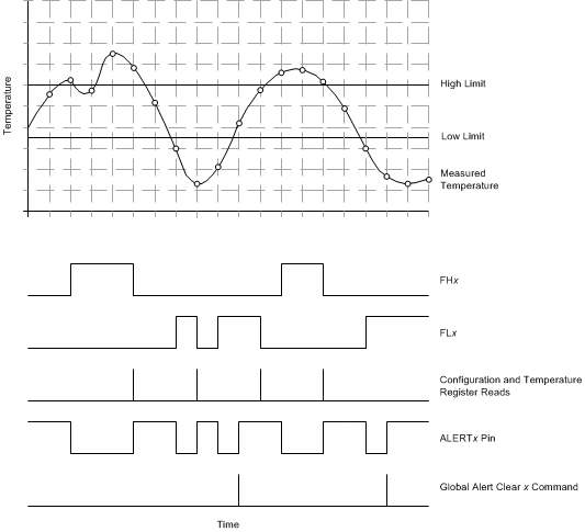
In alert mode (Tx/Ax = 0, default), the high and low limits form a temperature window. At the end of a conversion, if the temperature result exceeds the high limit or is less than the low limit, the respective flag (either FHx or FLx) and the ALERTx pin are asserted. If the alert outputs of multiple TMP107s are connected together, the TMP107 tripped alerts are still identifiable. To clear the ALERTx pin, issue a global alert clear x command, or read the configuration register as shown in Figure 16. To clear the FHx or FLx flag, read the configuration register. Alert-mode operation is shown in Figure 16.
 Figure 16. ALERTx Pin Behavior in Alert Mode (POLx = 0)
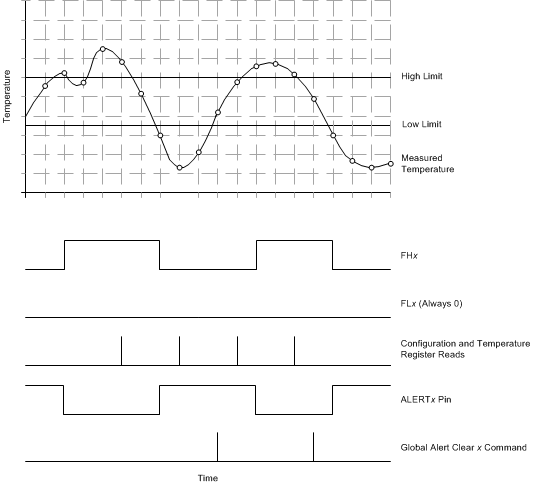
 In therm mode (Tx/Ax = 1), the high and low limits are used to form an upper-limit threshold detector. If the temperature result exceeds the high limit, the FHx flag and the ALERTx pin are asserted. The FHx flag and the ALERTx pin are then deasserted only after the temperature falls below the low limit. In therm mode, only the FHx flag is active. The FLx flag always reads 0. In therm mode, ALERTx and the flags are asserted and deasserted only at the end of a conversion and cannot be cleared by a configuration register read or global alert clear x command. Figure 17 shows therm-mode operation.
 Figure 17. ALERTx Pin Behavior in Therm Mode (POLx = 0)
 The limit registers default values are programmed in the EEPROM, and are acquired during power up or reset. The values can be dynamically changed by writing to the register. Disable alert and flag functionality by programming the high limit register to the highest temperature (7FFCh) and the low limit register to the lowest temperature (8000h). When disabled, the alert pins can still be controlled by polarity bits POL1 and POL2 (bit 7 and bit 3, respectively, in the configuration register) so that they work like general-purpose outputs (GPOs).