ZHCSQR8A March   2023  – December 2023 TMAG5170D-Q1

PRODUCTION DATA  

  1.   1
  2. 特性
  3. 应用
  4. 说明
  5. Pin Configuration and Functions
  6. Specifications
    1. 5.1 Absolute Maximum Ratings
    2. 5.2 ESD Ratings
    3. 5.3 Recommended Operating Conditions
    4. 5.4 Thermal Information
    5. 5.5 Electrical Characteristics
    6. 5.6 Magnetic Characteristics
    7. 5.7 Power up Timing
    8. 5.8 SPI Interface Timing
    9. 5.9 Typical Characteristics
  7. Detailed Description
    1. 6.1 Overview
    2. 6.2 Functional Block Diagram
    3. 6.3 Feature Description
      1. 6.3.1 Magnetic Flux Direction
      2. 6.3.2 Sensor Location
      3. 6.3.3 Magnetic Range Selection
      4. 6.3.4 Update Rate Settings
      5. 6.3.5 ALERT Function
        1. 6.3.5.1 Interrupt and Trigger Mode
        2. 6.3.5.2 Magnetic Switch Mode
      6. 6.3.6 Threshold Count
      7. 6.3.7 Diagnostics
        1. 6.3.7.1  Memory Cyclic Redundancy Check (CRC)
        2. 6.3.7.2  ALERT Integrity Check
        3. 6.3.7.3  VCC Check
        4. 6.3.7.4  Internal LDO Undervoltage Check
        5. 6.3.7.5  Digital Core Power-On Reset Check
        6. 6.3.7.6  SDO Output Check
        7. 6.3.7.7  Communication Cyclic Redundancy Check (CRC)
        8. 6.3.7.8  Oscillator Integrity Check
        9. 6.3.7.9  Magnetic Field Threshold Check
        10. 6.3.7.10 Temperature Alert Check
        11. 6.3.7.11 Analog Front-End (AFE) Check
        12. 6.3.7.12 Hall Resistance and Switch Matrix Check
        13. 6.3.7.13 Hall Offset Check
        14. 6.3.7.14 ADC Check
    4. 6.4 Device Functional Modes
      1. 6.4.1 Operating Modes
        1. 6.4.1.1 Active Mode
        2. 6.4.1.2 Standby Mode
        3. 6.4.1.3 Configuration Mode (DEFAULT)
        4. 6.4.1.4 Sleep Mode
        5. 6.4.1.5 Wake-Up and Sleep Mode
        6. 6.4.1.6 Deep-Sleep Mode
    5. 6.5 Programming
      1. 6.5.1 Data Definition
        1. 6.5.1.1 Magnetic Sensor Data
        2. 6.5.1.2 Temperature Sensor Data
        3. 6.5.1.3 Magnetic Sensor Offset Correction
        4. 6.5.1.4 Angle and Magnitude Data Definition
      2. 6.5.2 Serial Peripheral Interface (SPI)
        1. 6.5.2.1 SCK
        2. 6.5.2.2 CS
        3. 6.5.2.3 SDI
        4. 6.5.2.4 SDO
          1. 6.5.2.4.1 Regular 32-Bit SDO Read
          2. 6.5.2.4.2 Special 32-Bit SDO Read
        5. 6.5.2.5 SPI CRC
        6. 6.5.2.6 SPI Frame
          1. 6.5.2.6.1 32-Bit Read Frame
          2. 6.5.2.6.2 32-Bit Write Frame
  8. Application and Implementation
    1. 7.1 Application Information
      1. 7.1.1 Selecting the Sensitivity Option
      2. 7.1.2 Temperature Compensation for Magnets
      3. 7.1.3 Sensor Conversion
        1. 7.1.3.1 Continuous Conversion
        2. 7.1.3.2 Trigger Conversion
        3. 7.1.3.3 Pseudo-Simultaneous Sampling
      4. 7.1.4 Error Calculation During Linear Measurement
      5. 7.1.5 Error Calculation During Angular Measurement
    2. 7.2 Typical Application
      1. 7.2.1 Design Requirements
        1. 7.2.1.1 Gain Adjustment for Angle Measurement
      2. 7.2.2 Detailed Design Procedure
      3. 7.2.3 Application Curves
    3. 7.3 Best Design Practices
    4. 7.4 Power Supply Recommendations
    5. 7.5 Layout
      1. 7.5.1 Layout Guidelines
      2. 7.5.2 Layout Example
  9. Register Map
  10. Device and Documentation Support
    1. 9.1 接收文档更新通知
    2. 9.2 支持资源
    3. 9.3 Trademarks
    4. 9.4 静电放电警告
    5. 9.5 术语表
  11. 10Revision History
  12. 11Mechanical, Packaging, and Orderable Information

封装选项

机械数据 (封装 | 引脚)
散热焊盘机械数据 (封装 | 引脚)
订购信息

SPI CRC

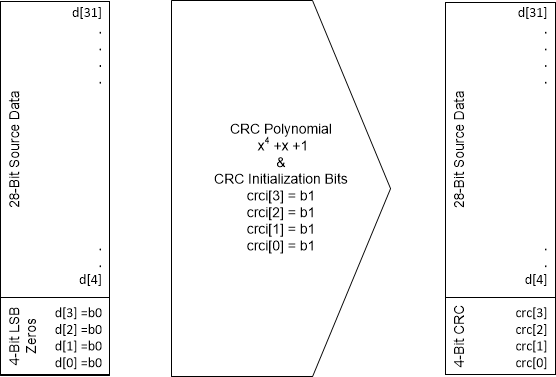
The TMAG5170D-Q1 performs mandatory CRC for SPI communication. The data integrity is maintained in both directions by a 4-bit CRC covering the content of the incoming and outgoing 32-bit messages. The four LSB bits of each 32-bit SPI frame are dedicated for the CRC. The CRC code is generated by the polynomial x4 + x + 1. Initialize the CRC bits with b1111.

During the SDI write frame, the TMAG5170D-Q1 reads for the CRC data before executing a write instruction. The write instruction from the controller is ignored if there is any CRC error present in the frame. During the SDI regular read frame, the TMAG5170D-Q1 starts to deliver the requested data through SDO line in the same frame and notifies the controller of any error occurrence through the ERROR_STAT bit. If the device detects a CRC error in the SDI line, the device will invert the last bit of the SDO CRC in the same frame to promptly signal to a controller that the SPI communication is compromised. A controller can also determine the presence of a CRC error in the SDI frame by checking the Status11 bit in the next regular read frame.
Note: The TMAG5170D-Q1 default mode at power up is CRC-enabled. With CRC enabled, the device will ignore all the SDI commands if proper CRC codes are not received. To disable the CRC at the SDI line, send the SPI SDI command x0F000407.
GUID-E72B4345-26F2-4F06-B2AF-2B88923CA2B0-low.gif Figure 6-9 4-Bit CRC Calculation

Use the following XOR function equations to calculate the 4-bit CRC. Figure 6-9 describes the notations of these equations.

Equation 3. c r c [ 0 ]   =   d [ 30 ]   ^   d [ 26 ]   ^   d [ 25 ]   ^   d [ 24 ]   ^   d [ 23 ]   ^   d [ 21 ]   ^   d [ 19 ]   ^   d [ 18 ]   ^   d [ 15 ]   ^   d [ 11 ]   ^   d [ 10 ]   ^   d [ 9 ]   ^   d [ 8 ]   ^   d [ 6 ]   ^   d [ 4 ]   ^   d [ 3 ]   ^   d [ 0 ]   ^   c r c i [ 2 ]
Equation 4. c r c [ 1 ]   =   d [ 31 ]   ^   d [ 30 ]   ^   d [ 27 ]   ^   d [ 23 ]   ^   d [ 22 ]   ^   d [ 21 ]   ^   d [ 20 ]   ^   d [ 18 ]   ^   d [ 16 ]   ^   d [ 15 ]   ^   d [ 12 ]   ^   d [ 8 ]   ^   d [ 7 ]   ^   d [ 6 ]   ^   d [ 5 ]   ^   d [ 3 ]   ^   d [ 1 ]   ^   d [ 0 ]   ^   c r c i [ 2 ]   ^   c r c i [ 3 ]
Equation 5. c r c [ 2 ]   =   d [ 31 ]   ^   d [ 28 ]   ^   d [ 24 ]   ^   d [ 23 ]   ^   d [ 22 ]   ^   d [ 21 ]   ^   d [ 19 ]   ^   d [ 17 ]   ^   d [ 16 ]   ^   d [ 13 ]   ^   d [ 9 ]   ^   d [ 8 ]   ^   d [ 7 ]   ^   d [ 6 ]   ^   d [ 4 ]   ^   d [ 2 ]   ^   d [ 1 ]   ^   c r c i [ 0 ]   ^   c r c i [ 3 ]
Equation 6. c r c [ 3 ]   =   d [ 29 ]   ^   d [ 25 ]   ^   d [ 24 ]   ^   d [ 23 ]   ^   d [ 22 ]   ^   d [ 20 ]   ^   d [ 18 ]   ^   d [ 17 ]   ^   d [ 14 ]   ^   d [ 10 ]   ^   d [ 9 ]   ^   d [ 8 ]   ^   d [ 7 ]   ^   d [ 5 ]   ^   d [ 3 ]   ^   d [ 2 ]   ^   c r c i [ 1 ]

The following shows example codes for calculating the 4-bit CRC.

function logic [3:0] calculate_crc4;
   input logic [27:0] frame;

   logic [31:0]       padded_frame;
   logic [3:0] 	      frame_crc;
   logic 	      inv;
   integer 	      i;

   padded_frame = {frame, 4'b0000};
   
   begin
      frame_crc = 4'hf; // initial value
      for (i=31; i >= 0; i=i-1) begin
	 inv = padded_frame[i] ^ frame_crc[3];
	 frame_crc[3] = frame_crc[2];
	 frame_crc[2] = frame_crc[1];
	 frame_crc[1] = frame_crc[0] ^ inv;
	 frame_crc[0] = inv;
      end
      return frame_crc;
   end
endfunction