ZHCSI89C November   2017  – March 2024 TLV755P

PRODUCTION DATA  

  1.   1
  2. 特性
  3. 应用
  4. 说明
  5. Pin Configuration and Functions
  6. Specifications
    1. 5.1 Absolute Maximum Ratings
    2. 5.2 ESD Ratings
    3. 5.3 Recommended Operating Conditions
    4. 5.4 Thermal Information
    5. 5.5 Electrical Characteristics
    6. 5.6 Typical Characteristics
  7. Detailed Description
    1. 6.1 Overview
    2. 6.2 Functional Block Diagram
    3. 6.3 Feature Description
      1. 6.3.1 Undervoltage Lockout (UVLO)
      2. 6.3.2 Enable (EN)
      3. 6.3.3 Internal Foldback Current Limit
      4. 6.3.4 Thermal Shutdown
    4. 6.4 Device Functional Modes
      1. 6.4.1 Normal Operation
      2. 6.4.2 Dropout Operation
      3. 6.4.3 Disabled
  8. Application and Implementation
    1. 7.1 Application Information
      1. 7.1.1 Input and Output Capacitor Selection
      2. 7.1.2 Dropout Voltage
      3. 7.1.3 Exiting Dropout
      4. 7.1.4 Reverse Current
      5. 7.1.5 Power Dissipation (PD)
        1. 7.1.5.1 Estimating Junction Temperature
    2. 7.2 Typical Application
      1. 7.2.1 Design Requirements
      2. 7.2.2 Detailed Design Procedure
        1. 7.2.2.1 Input Current
        2. 7.2.2.2 Thermal Dissipation
      3. 7.2.3 Application Curve
    3. 7.3 Power Supply Recommendations
    4. 7.4 Layout
      1. 7.4.1 Layout Guidelines
      2. 7.4.2 Layout Examples
  9. Device and Documentation Support
    1. 8.1 Device Support
      1. 8.1.1 Device Nomenclature
    2. 8.2 接收文档更新通知
    3. 8.3 支持资源
    4. 8.4 Trademarks
    5. 8.5 静电放电警告
    6. 8.6 术语表
  10. Revision History
  11. 10Mechanical, Packaging, and Orderable Information

封装选项

请参考 PDF 数据表获取器件具体的封装图。

机械数据 (封装 | 引脚)
  • DYD|5
  • DBV|5
  • DQN|4
  • DRV|6
散热焊盘机械数据 (封装 | 引脚)
订购信息

Typical Characteristics

at operating temperature TJ = 25°C, VIN = VOUT(NOM) + 0.5V or 1.45V (whichever is greater), IOUT = 1mA, VEN = VIN, and CIN = COUT = 1µF (unless otherwise noted)
GUID-C62E7D4A-2DDD-47C0-835C-A52FA3090638-low.gif
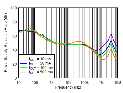
VIN = 4.3V, VOUT = 3.3V, COUT = 1µF
Figure 5-1 PSRR vs Frequency and IOUT
GUID-CF465040-0A76-42E6-AEFF-99DE4694F5C9-low.gif
VIN = 4.3V, VOUT = 3.3V, IOUT = 500mA
Figure 5-3 PSRR vs Frequency and COUT
GUID-1089D93B-E79C-4604-ABC5-AB43CFF708D3-low.gif
VOUT = 3.3V, IOUT = 500mA, COUT = 1µF, VRMS BW = 10Hz to 100kHz
Figure 5-5 Output Spectral Noise Density vs Frequency and IOUT
GUID-F2087031-7390-47AF-AEBD-6B894147DE3C-low.gif
VOUT = 3.3V, COUT = 1µF, VIN slew rate = 1V/µs
Figure 5-7 Line Transient
GUID-A3596FC3-B6B9-414D-9F1D-7D524B5E885C-low.gif
 
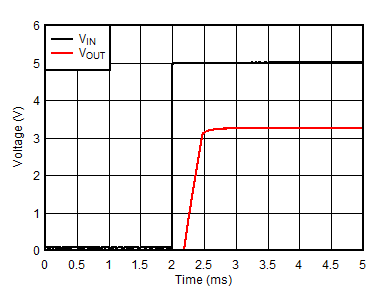
Figure 5-9 VIN = VEN Power-Up
GUID-20001946-77D1-4394-9BD6-6497B26563CA-low.gif
VIN = 5V, IOUT = 100mA, VEN slew rate = 1V/µs,
VOUT = 3.3V
Figure 5-11 EN Start-Up
GUID-2764F4A4-018D-4462-886D-E3F6E9C1C74C-low.gif
 
Figure 5-13 3.3V Dropout Voltage vs IOUT
GUID-6174BFC6-38F0-414E-A9FE-CF4E89528902-low.gif
VOUT = 3.3V, IOUT = 1mA
Figure 5-15 3.3V Regulation vs VIN (Line Regulation)
GUID-DBA2F2C5-6244-4055-8DA7-F4AEF120BEF7-low.gif
 
Figure 5-17 IGND vs IOUT
GUID-43AADF91-C23D-4A85-BA21-5B774EF1D61F-low.gif
VOUT = 3.3V, IOUT = 0mA
Figure 5-19 IQ vs VIN
GUID-25239783-6429-4022-ABB0-01783C069001-low.gif
VEN = 0V
Figure 5-21 ISHDN vs Temperature
GUID-370CA781-F7E0-44AA-9509-998BD7E5F0CF-low.gif
VEN = 5.5V
Figure 5-23 IEN vs VIN
GUID-BA9F04A6-A36B-4176-AF03-3BBABE9CDB74-low.gif
 
Figure 5-25 VOUT vs IOUT Pulldown Resistor
GUID-4E067C73-CE10-4DAD-8E85-E32587517696-low.gif
VOUT = 3.3V, COUT = 1µF, IOUT = 500mA
Figure 5-2 PSRR vs Frequency and VIN
GUID-DD4CE187-2333-4171-A1C7-39C3C56DA606-low.gif
VOUT = 3.3V, VRMS BW = 10Hz to 100kHz
Figure 5-4 Output Spectral Noise Density vs Frequency and COUT
GUID-FABF9B1F-075E-4FA9-8835-B0F0FC8976C9-low.gif
IOUT = 500mA, COUT = 1µF, VRMS BW = 10Hz to 100kHz
 
Figure 5-6 Output Noise Voltage vs VOUT
GUID-13FC6E75-42E7-44C8-BCB0-2CA13CA76A62-low.gif
VIN = 5V, VOUT = 3.3V, COUT = 1µF, IOUT slew rate = 1A/µs
Figure 5-8 3.3V, 1mA to 500mA Load Transient
GUID-E8DBBA33-2908-402E-B8F1-51E1B130C6C5-low.gif
 
Figure 5-10 VIN = VEN Shutdown
GUID-C566E36A-D14D-49C7-8FD1-FA8DBBD924A4-low.gif
 
 
Figure 5-12 Load Regulation vs IOUT
GUID-9D559D53-1880-4B2D-B020-FB9FA5D85DB8-low.gif
 
Figure 5-14 5.0V Dropout Voltage vs IOUT
GUID-9578E539-3F95-4D3D-9210-FB1E981A915A-low.gif
IOUT = 1mA, VOUT = 5V
Figure 5-16 5.0V Accuracy vs VIN (Line Regulation)
GUID-CC03CFD6-B5FC-4195-BE2D-DE5533047752-low.gif
VOUT = 3.3V, IOUT = 1mA
Figure 5-18 IGND vs VIN
GUID-5520B30F-6280-43AA-9CA0-57B1A5813831-low.gif
VEN = 0V
Figure 5-20 ISHDN vs VIN
GUID-3ABE6388-4734-4055-8550-EF231D04EC04-low.gif
 
Figure 5-22 Enable Threshold vs Temperature
GUID-C95CA115-CD0A-474A-A3CB-4E29310703B3-low.gif
 
Figure 5-24 UVLO Threshold vs Temperature
GUID-CF648830-DD18-4EBF-AA7B-5DBF664240D4-low.gif
 
Figure 5-26 3.3V Foldback Current Limit, VOUT vs IOUT