ZHCSJ63 December 2018 TLV1805
PRODUCTION DATA.
- 1 特性
- 2 应用
- 3 说明
- 4 修订历史记录
- 5 说明 (续)
- 6 Pin Configuration and Functions
- 7 Specifications
- 8 Detailed Description
-
9 Application and Implementation
- 9.1 Application Information
- 9.2 Typical Applications
- 10Power Supply Recommendations
- 11Layout
- 12器件和文档支持
- 13机械、封装和可订购信息
9.2.6 P-Channel Reverse Current Protection With Overvotlage Protection
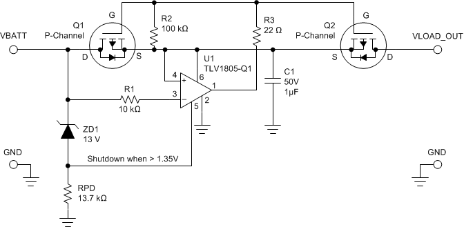
The SHDN pin can be utilized to add Overvotlage Protection (OVP) by adding a second MOSFET, zener diode and resistor, as shown in Figure 71.
 Figure 71. Adding Overvoltage Protection Using SHDN Pin
 When the SHDN pin is pulled 1.35 V above V-, the comparator is placed in shutdown. During shutdown, the comparator output goes Hi-Z and R2 pulls the gate and source together to turn off the MOSFET (VGS = 0 V).
RPD pulls the SHDN pin low while the Zener diode is not conducting (< VZ). When ZD1 reaches its breakdown voltage and starts conducting, it will pull RPD up to a voltage calculated to place >1.35 V on the shutdown pin.
The Zener diode ZD1 should be chosen so that the breakdown voltage (VB) is 1.35 V below the desired overvoltage point. The Zener should have low sub-threshold leakage and a sharp knee, such as the low power 1N47xx or BZD series.
The pull-down resistor RPD should be chosen to create 1.35 V at the desired Zener diode current (usually 100uA to 1mA) at the Zener breakdown voltage. Actual resistor value should be verified on the bench due to differences in actual Zener diode threshold voltages.
If a 14.3 V overvotlage trip point (OVP) is desired, the Zener Diode voltage should be 12.95 V. We will choose a 100uA Zener current. The required Zener diode breakdown voltage is determined from:
Resistor RPD may be split into two resistors to create a voltage divider if more precise trip points are needed, or a more convenient zener voltage is desired. Series voltage references can also be used if more accuracy is desired. A second resistor in series with the Zener or reference can extend the breakdown voltage.
The maximum voltage allowed on the Shutdown pin is 5.5V, so make sure the highest VBATT voltage does not exceed 5.5 V.
Note that the above circuit, as shown for simplicity, does not protect against reverse voltage. Reverse clamping diodes would be needed on the -IN, SHDN and Load Output. Also make sure VBATT does not exceed the VGS(MAX) of the MOSFET.