ZHCSJ63 December 2018 TLV1805
PRODUCTION DATA.
- 1 特性
- 2 应用
- 3 说明
- 4 修订历史记录
- 5 说明 (续)
- 6 Pin Configuration and Functions
- 7 Specifications
- 8 Detailed Description
-
9 Application and Implementation
- 9.1 Application Information
- 9.2 Typical Applications
- 10Power Supply Recommendations
- 11Layout
- 12器件和文档支持
- 13机械、封装和可订购信息
9.2.4.2 N-Channel Reverse Current Protection Circuit
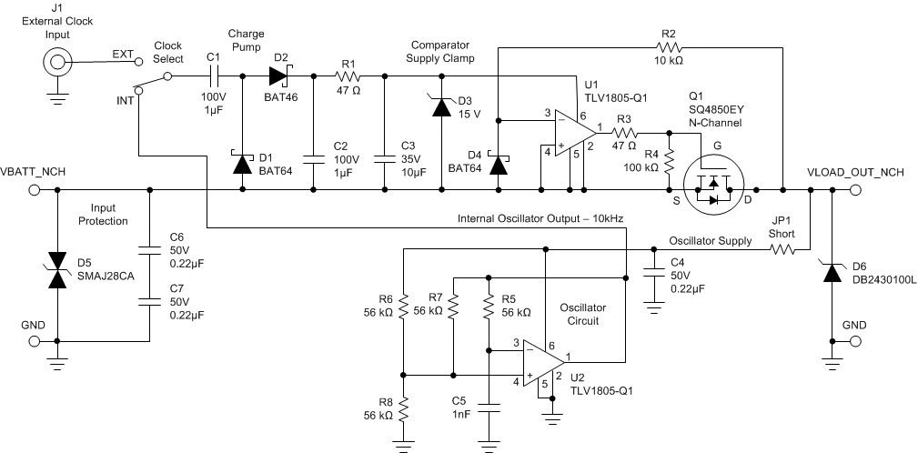
In order to turn "on" the N-Channel MOSFET, the MOSFET gate must be brought "High" above VBATT. If a higher voltage is not available, a charge pump circuit is required to provide the comparator with a supply voltage above VBATT.
 Figure 69. N-Channel Reverse Current Schematic with Oscillator
 C1, D1, D2 & C2 form the charge pump. The AC drive signal is applied through C1 into the charge pump. The result is a voltage across C2 that is approximately equal to the peak-to-peak amplitude of the AC waveform, minus 700mV. If a 12Vpp waveform is applied to the C1 input, 11.3V will be generated across C2. This voltage is on top of the VBATT voltage, so the voltage seen from the D2-C2 junction ground is 23.3V. This provides the needed higher voltage to drive the MOSFET and power the comparator.
An external oscillator source may be used, such as the gate drive output of a switcher, system clock or any avaialbe clock source in the 1kHz to 10MHz range. The charge pump should be fed by a 50 percent duty cycle square wave source of 5Vpp or more. Since the input capacitor of the charge-pump effectively AC-couples the input, the oscillator may be ground referenced.
R1 and D3 form the comparator supply clamp to limit the gate drive to prevent exceeding the VGS(MAX) of the MOSFET during an overvotlage event. R1 must be sized to dissapate any expected overvoltage.
D4 and R2 clamp the input should VBATT drop below VLOAD (as in a supply reversal).
The output diode D6 is used to anchor the output during light or floating loads. At light or no loads, there is a possibility the MOSFET could turn on due to the comparator offset voltage. The diode provides enough of a negative leakage to turn the MOSFET off.