ZHCSJ63 December   2018 TLV1805

PRODUCTION DATA.  

  1. 特性
  2. 应用
  3. 说明
    1.     Device Images
      1.      采用 P 沟道 MOSFET 的过压保护
      2.      采用 P 沟道 MOSFET 的反向电流和过压保护
  4. 修订历史记录
  5. 说明 (续)
  6. Pin Configuration and Functions
    1.     Pin Functions
  7. Specifications
    1. 7.1 Absolute Maximum Ratings
    2. 7.2 ESD Ratings
    3. 7.3 Recommended Operating Conditions
    4. 7.4 Thermal Information
    5. 7.5 Electrical Characteristics
    6. 7.6 Switching Characteristics
    7. 7.7 Typical Characteristics
  8. Detailed Description
    1. 8.1 Overview
    2. 8.2 Functional Block Diagram
    3. 8.3 Feature Description
      1. 8.3.1 Rail to Rail Inputs
      2. 8.3.2 Power On Reset
      3. 8.3.3 High Power Push-Pull Output
      4. 8.3.4 Shutdown Function
      5. 8.3.5 Internal Hysteresis
    4. 8.4 Device Functional Modes
      1. 8.4.1 External Hysteresis
        1. 8.4.1.1 Inverting Comparator With Hysteresis
        2. 8.4.1.2 Noninverting Comparator With Hysteresis
  9. Application and Implementation
    1. 9.1 Application Information
    2. 9.2 Typical Applications
      1. 9.2.1 Design Requirements
      2. 9.2.2 Detailed Design Procedure
      3. 9.2.3 Application Curve
      4. 9.2.4 Reverse Current Protection Using MOSFET and TLV1805
        1. 9.2.4.1 Minimum Reverse Current
        2. 9.2.4.2 N-Channel Reverse Current Protection Circuit
          1. 9.2.4.2.1 N-Channel Oscillator Circuit
      5. 9.2.5 P-Channel Reverse Current Protection Circuit
      6. 9.2.6 P-Channel Reverse Current Protection With Overvotlage Protection
      7. 9.2.7 ORing MOSFET Controller
  10. 10Power Supply Recommendations
  11. 11Layout
    1. 11.1 Layout Guidelines
    2. 11.2 Layout Example
  12. 12器件和文档支持
    1. 12.1 文档支持
      1. 12.1.1 相关文档
    2. 12.2 接收文档更新通知
    3. 12.3 社区资源
    4. 12.4 商标
    5. 12.5 静电放电警告
    6. 12.6 术语表
  13. 13机械、封装和可订购信息

封装选项

机械数据 (封装 | 引脚)
散热焊盘机械数据 (封装 | 引脚)
订购信息

Typical Characteristics

at TA = 25°C, VS = 12 V, VCM = VS/2, and input overdrive = 100 mV (unless otherwise noted)
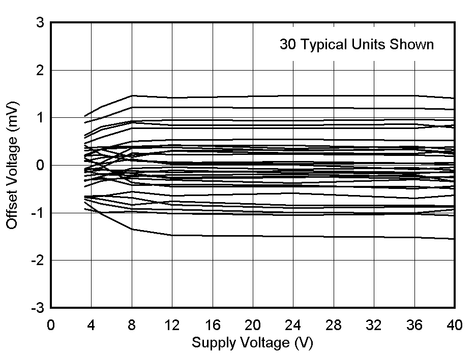
TLV1805 VIO_vs_VS.gif
Figure 3. Input Offset Voltage vs. Supply Voltage
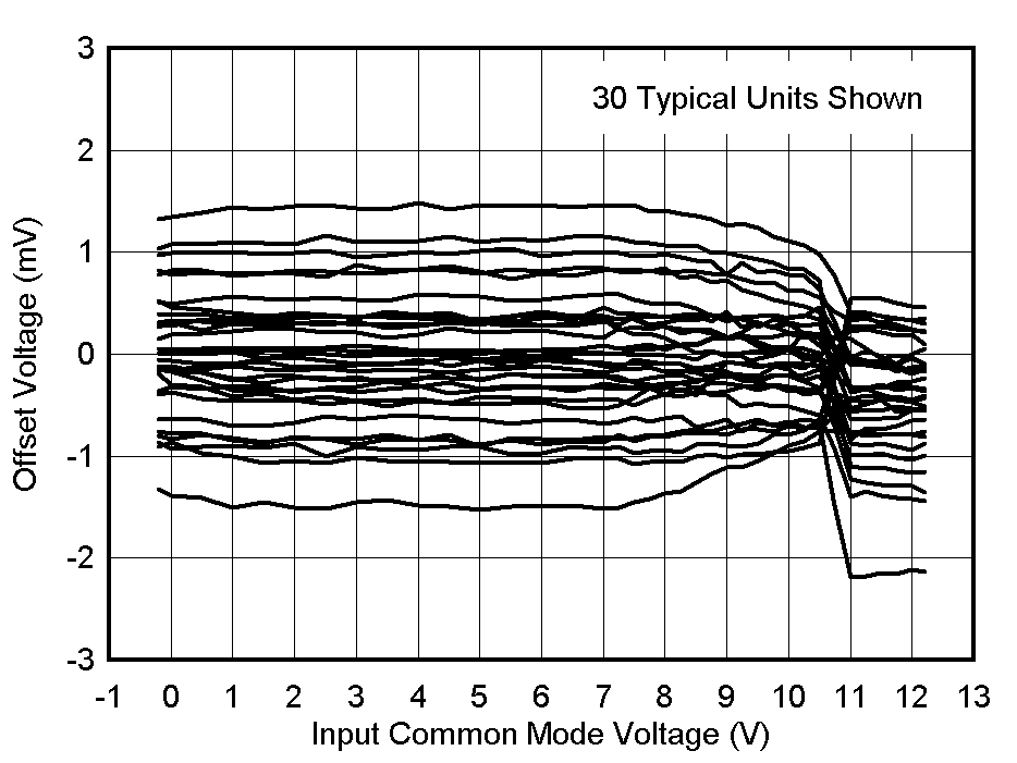
TLV1805 VIO_vs_VCM.gif
Figure 5. Offset Voltage vs. Common Mode
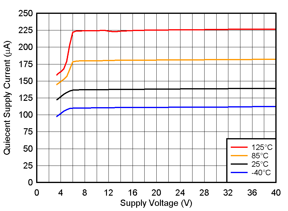
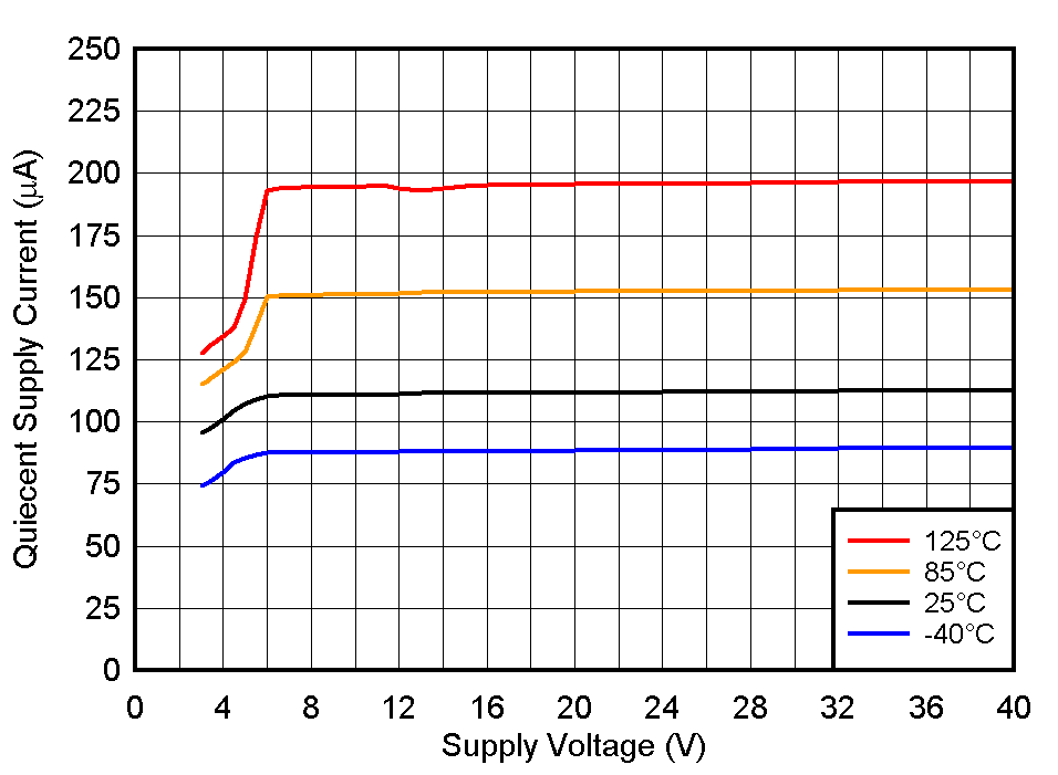
TLV1805 IQ_vs_VS.gif
VCM = V- Output Low (VID = -0.1 V)
Figure 7. Supply Current vs. Supply Voltage, Output Low
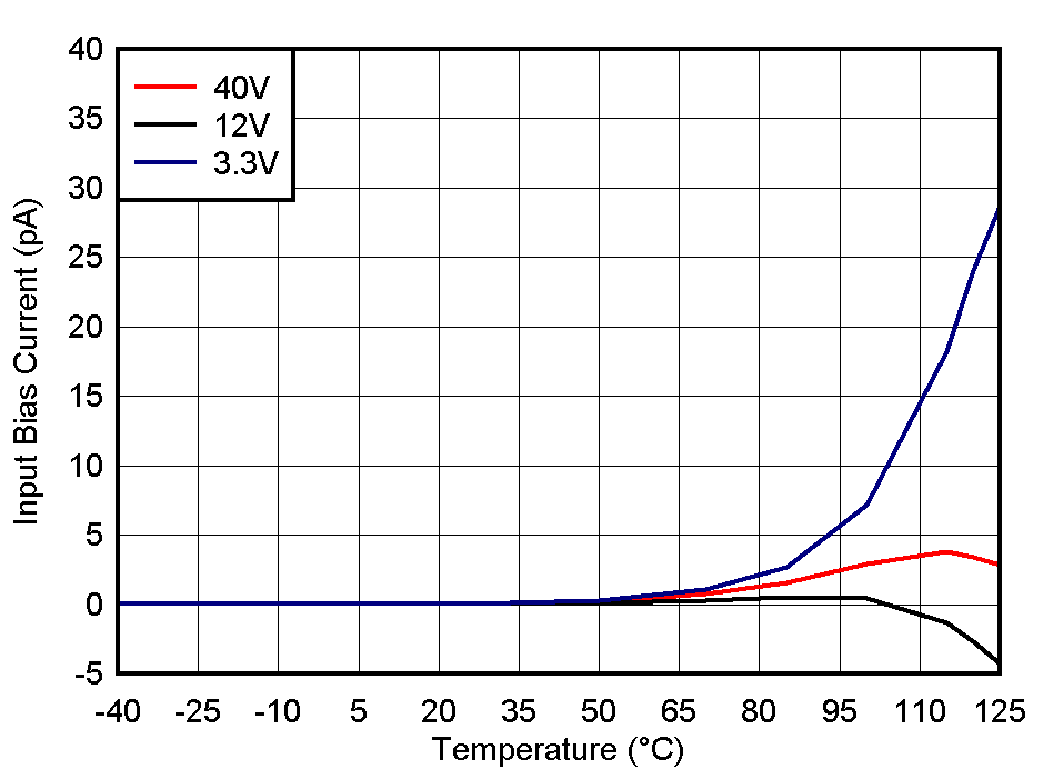
TLV1805 IB_vs_TA.gif
Figure 9. Input Bias Current vs. Temperature
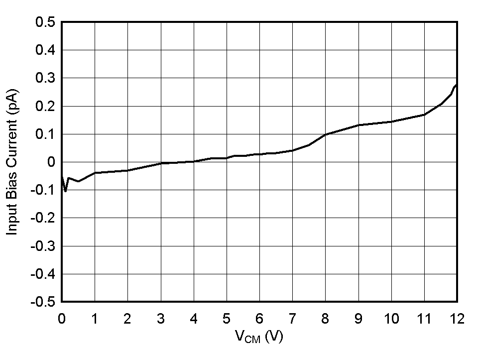
TLV1805 IB_vs_VCM_25C.gif
TA = 25 °C
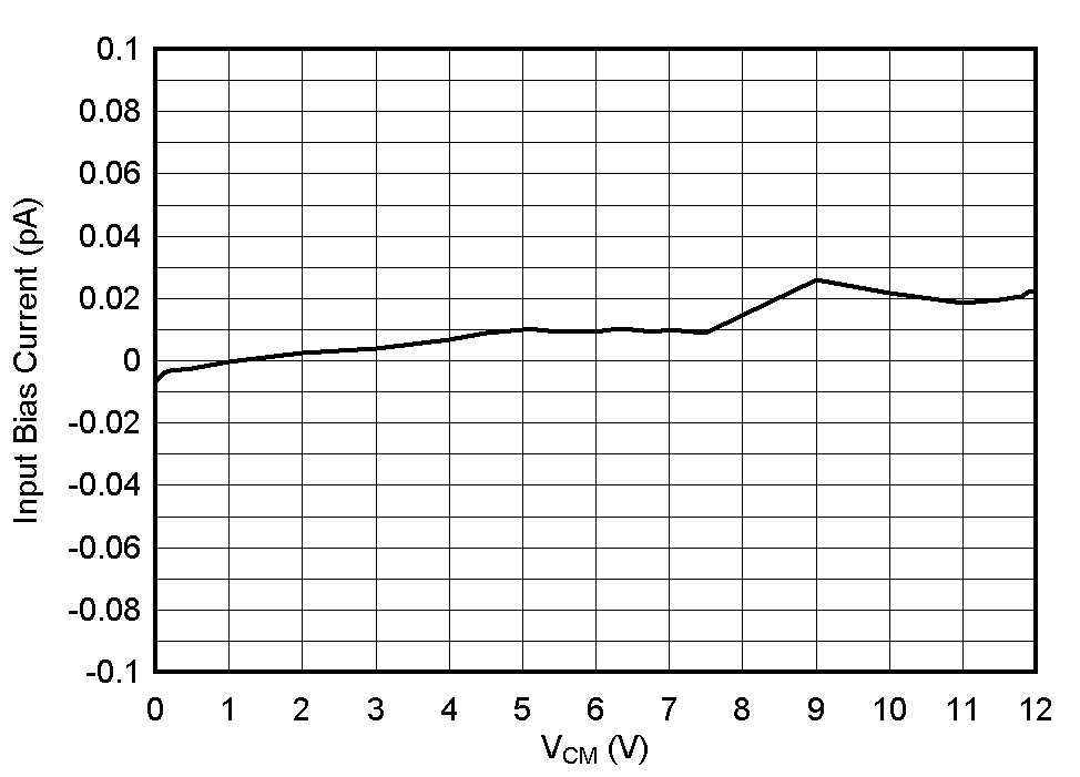
Figure 11. Input Bias Current vs. Common Mode, 25°C
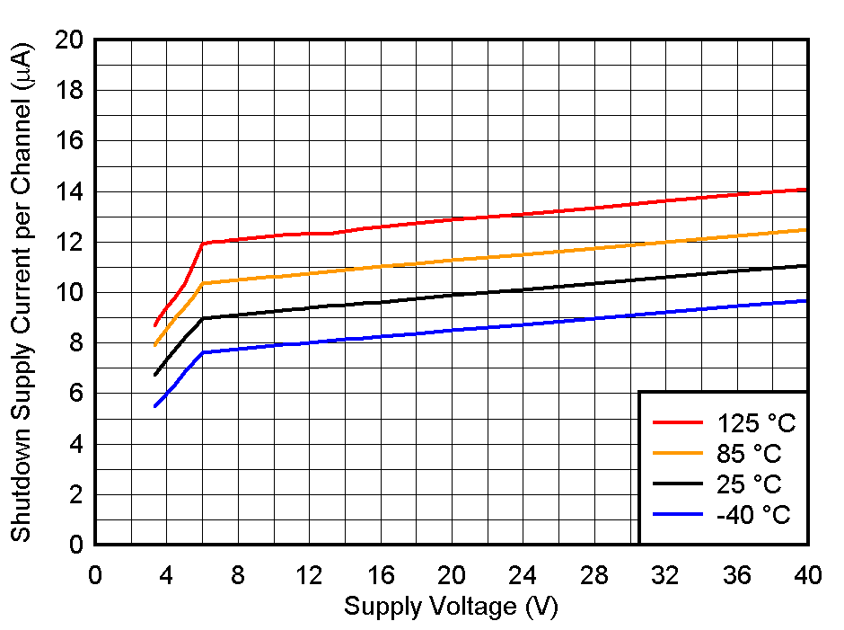
TLV1805 IQsd_vs_VS.gif
VCM = V-
Figure 13. Shutdown Supply Current vs. Supply Votlage
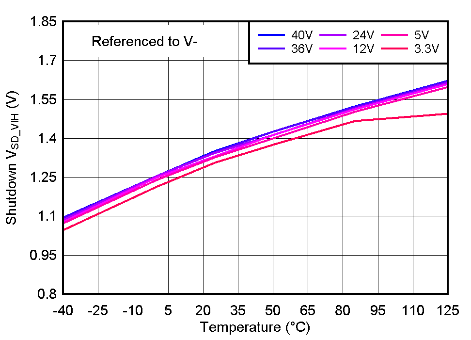
TLV1805 SDVHI_vs_TA.gif
Figure 15. Shutdown Voltage High Threshold vs. Temperature
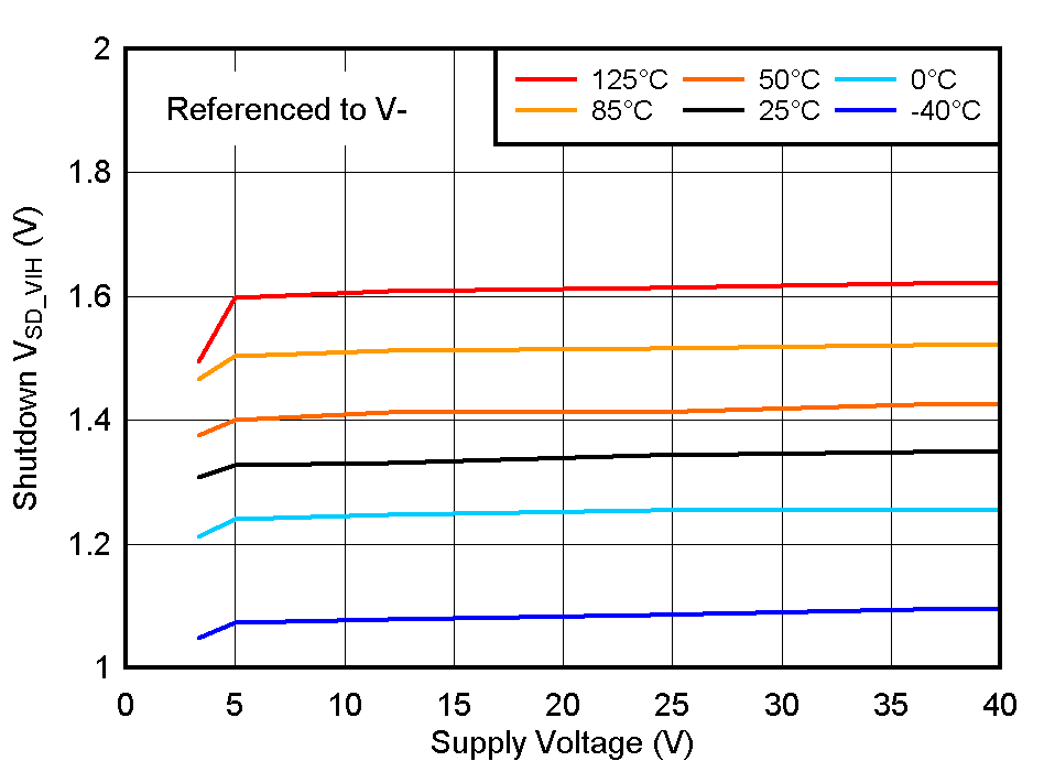
TLV1805 SDVHI_vs_VS.gif
Figure 17. Shutdown Voltage High Threshold vs. Supply Voltage
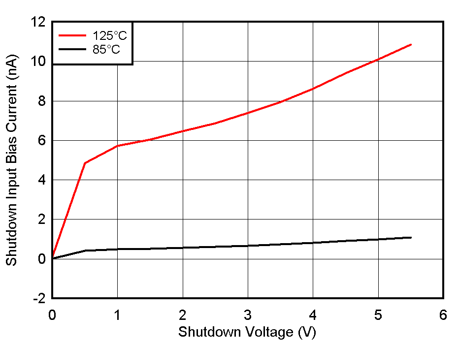
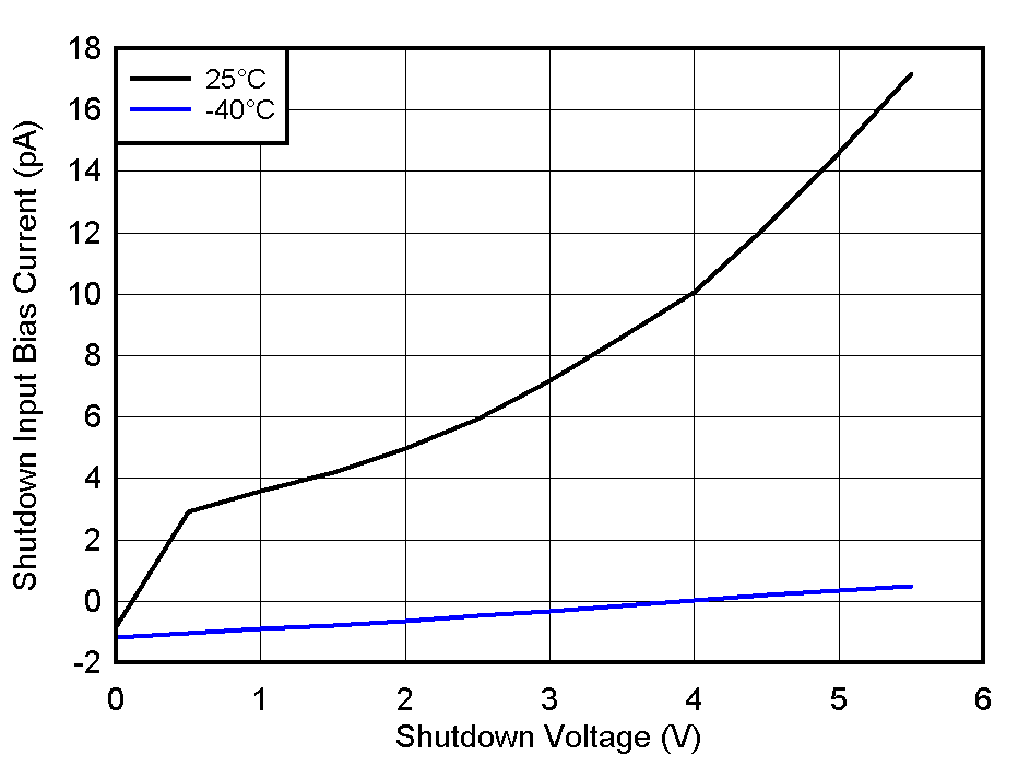
TLV1805 SDIB_vs_VSD_12V_125_85.gif
Figure 19. Shutdown Input Bias Current vs. Shutdown Input Voltage, High Temperatures
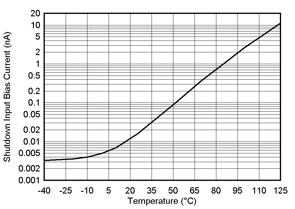
TLV1805 SDIB_vs_TA.gif
VSD = 5 V
Figure 21. Shutdown Input Bias Current vs. Temperature
TLV1805 VOH_vs_Vs.gif
ISOURCE = 1 mA
Figure 23. Output High Voltage vs. Supply Voltage
TLV1805 VOL_vs_IO_Vs3p3.gif
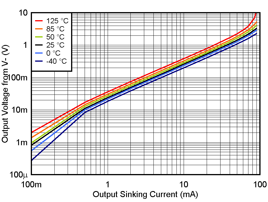
VS = 3.3 V
Figure 25. Output Sinking Current vs. Output Voltage
at 3.3V
TLV1805 VOL_vs_IO_Vs12.gif
VS = 12 V
Figure 27. Output Sinking Current vs. Output Voltage
at 12V
TLV1805 VOL_vs_IO_Vs40.gif
VS = 40 V
Figure 29. Output Sinking Current vs. Output Voltage
at 40V
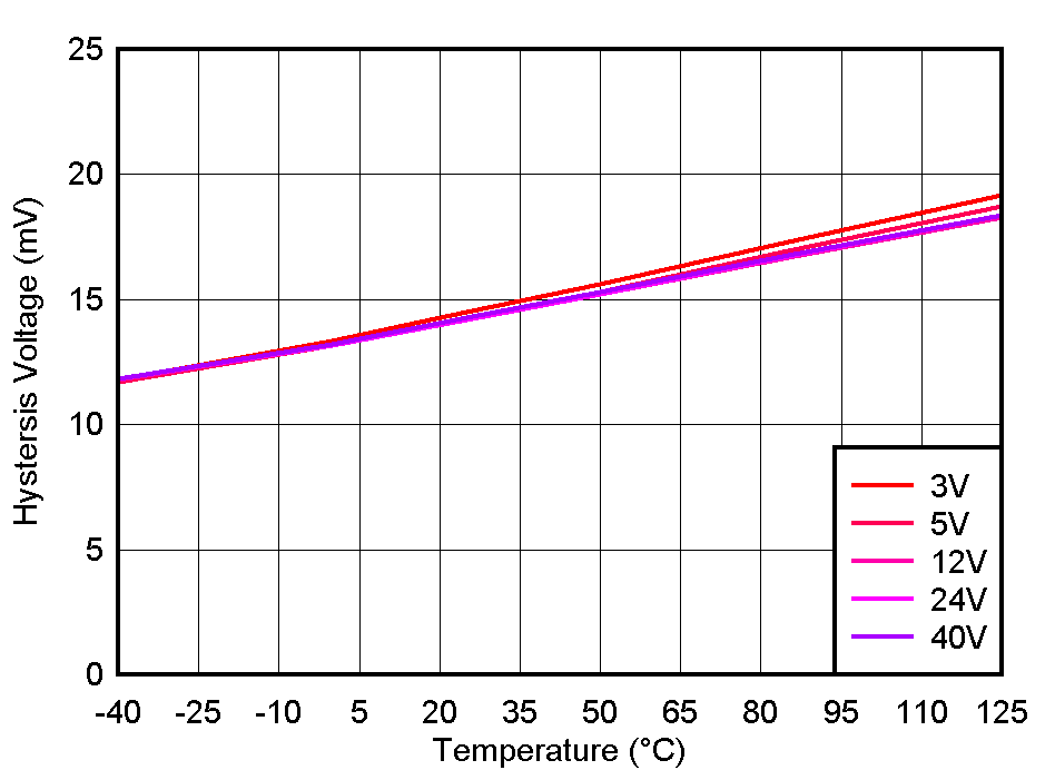
TLV1805 HYST_vs_TA.gif
Figure 31. Hysteresis vs. Temperature
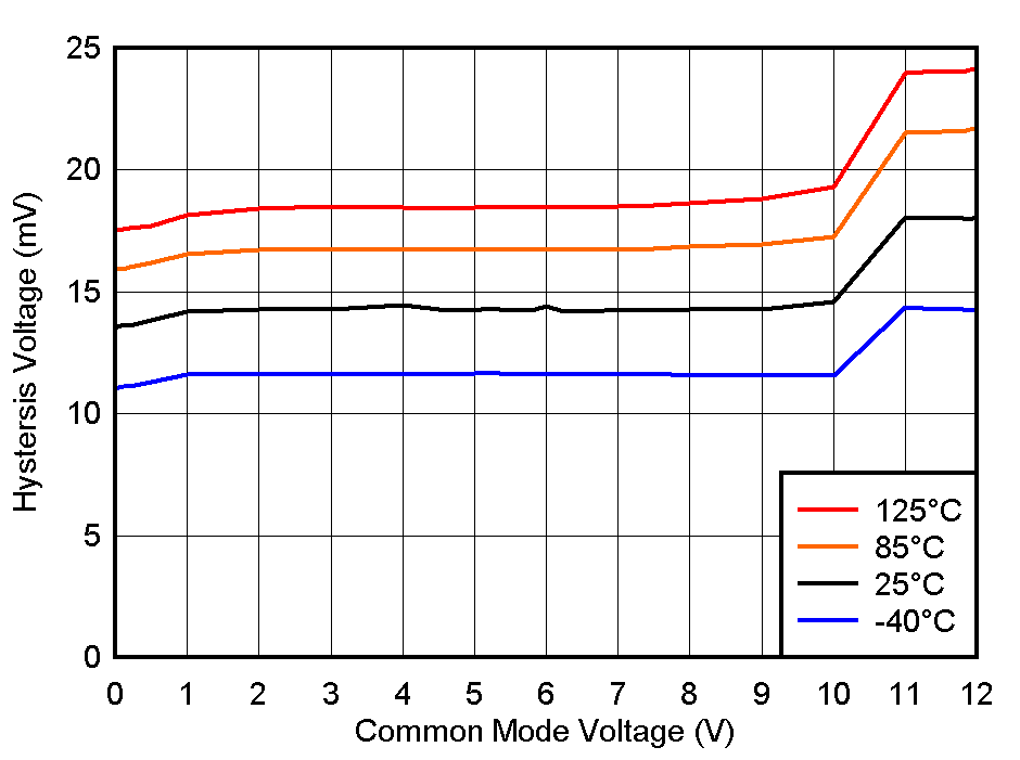
TLV1805 HYST_vs_VCM.gif
Figure 33. Hysteresis vs Common-Mode Voltage
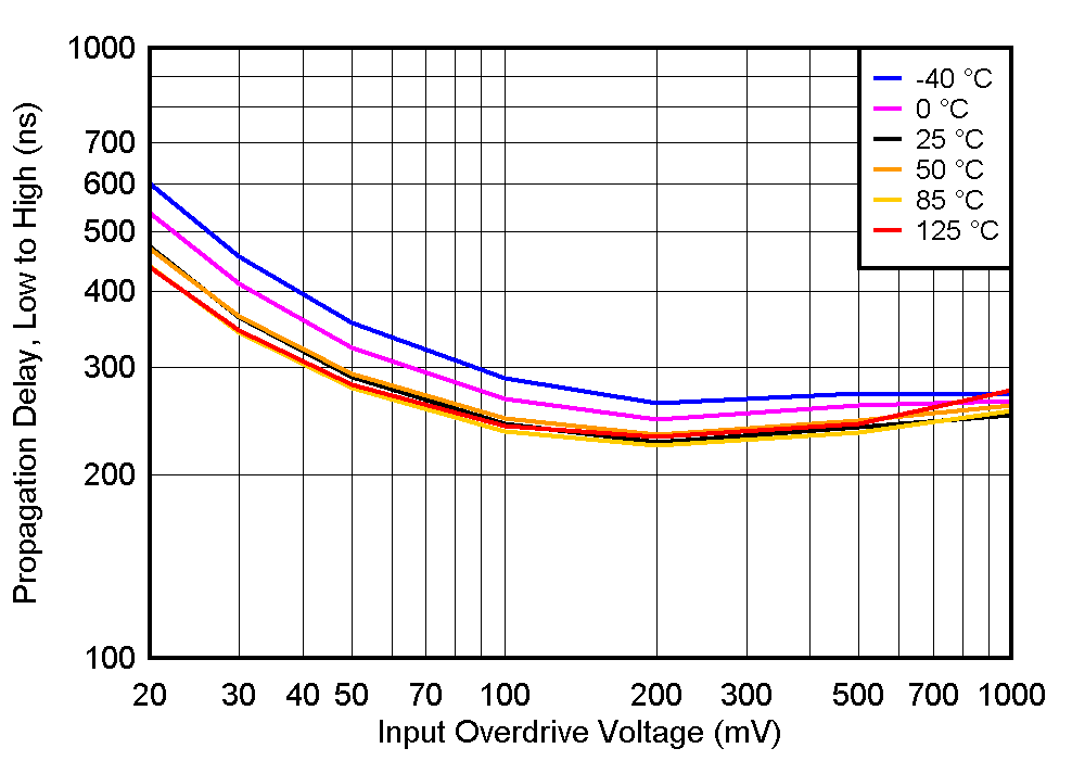
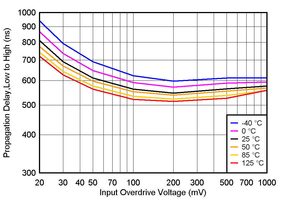
TLV1805 TPLH_vs_VOD_Vs3p3.gif
VS = 3.3 V CL = 15pF
Figure 35. TPLH Response Time vs. Overdrive
at 3.3V
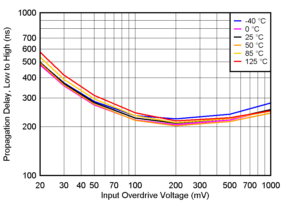
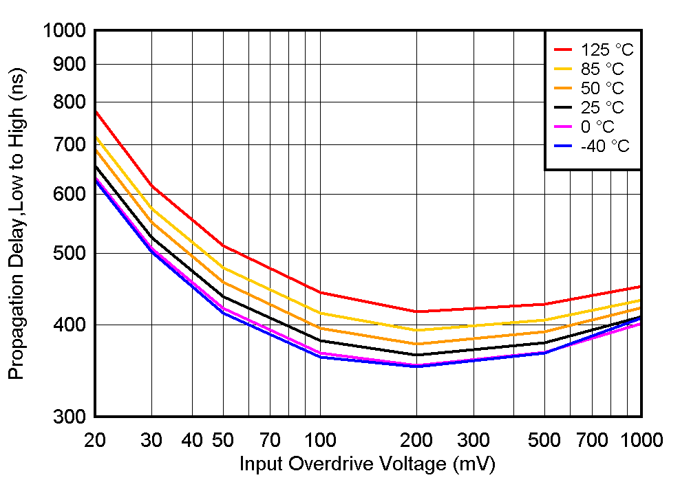
TLV1805 TPLH_vs_VOD_Vs5.gif
VS = 5 V CL = 15pF
Figure 37. TPLH Response Time vs. Overdrive
at 5V
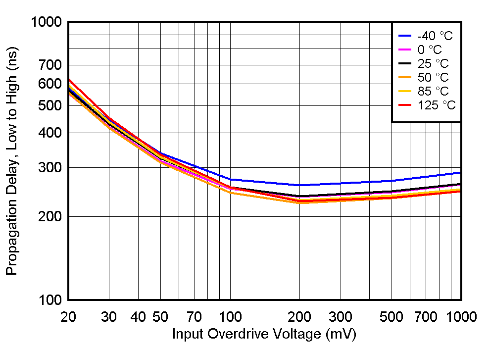
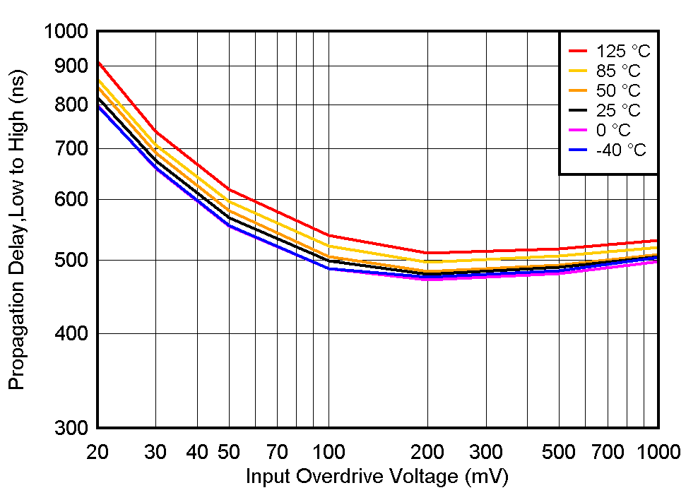
TLV1805 TPLH_vs_VOD_Vs12.gif
VS = 12 V CL = 15pF
Figure 39. TPLH Response Time vs.
Overdrive at 12V
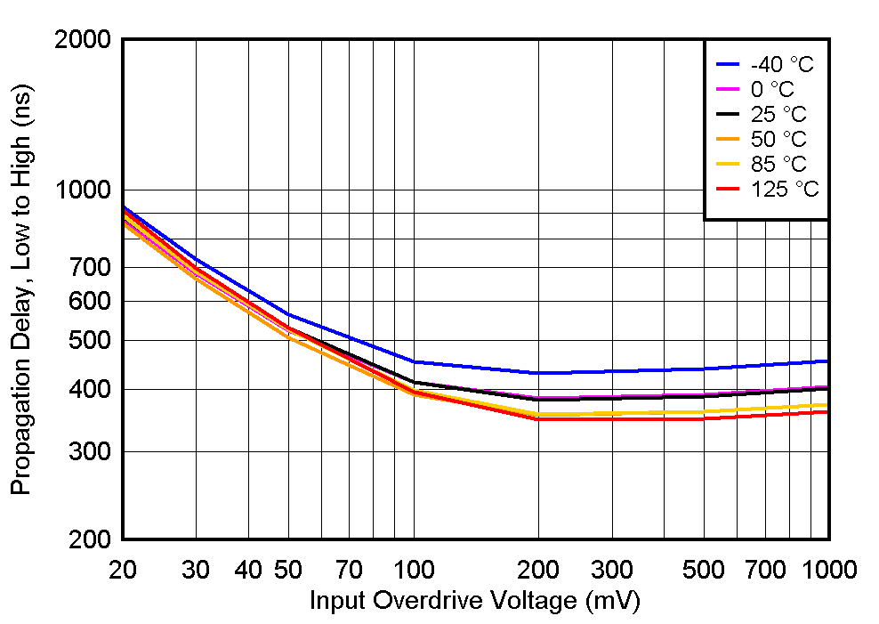
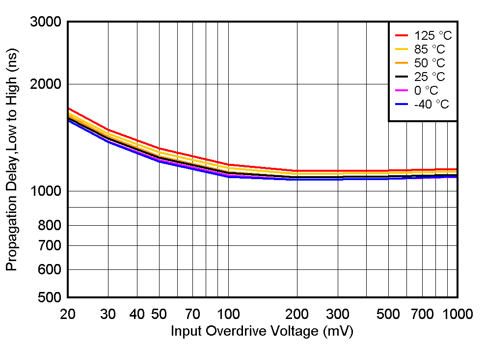
TLV1805 TPLH_vs_VOD_Vs40.gif
VS = 40 V CL = 15pF
Figure 41. TPLH Response Time vs. Overdrive
at 40V
TLV1805 TPLH_vs_VOD_Vs3p3_4n.gif
VS = 3.3 V CL = 4nF
Figure 43. TPLH Response Time vs. Overdrive
at 3.3V
TLV1805 TPLH_vs_VOD_Vs5_4n.gif
VS = 5 V CL = 4nF
Figure 45. TPLH Response Time vs. Overdrive
at 5V
TLV1805 TPLH_vs_VOD_Vs12_4n.gif
VS = 12 V CL = 4nF
Figure 47. TPLH Response Time vs.
Overdrive at 12V
TLV1805 TPLH_vs_VOD_Vs40_4n.gif
VS = 40 V CL = 4nF
Figure 49. TPLH Response Time vs. Overdrive
at 40V
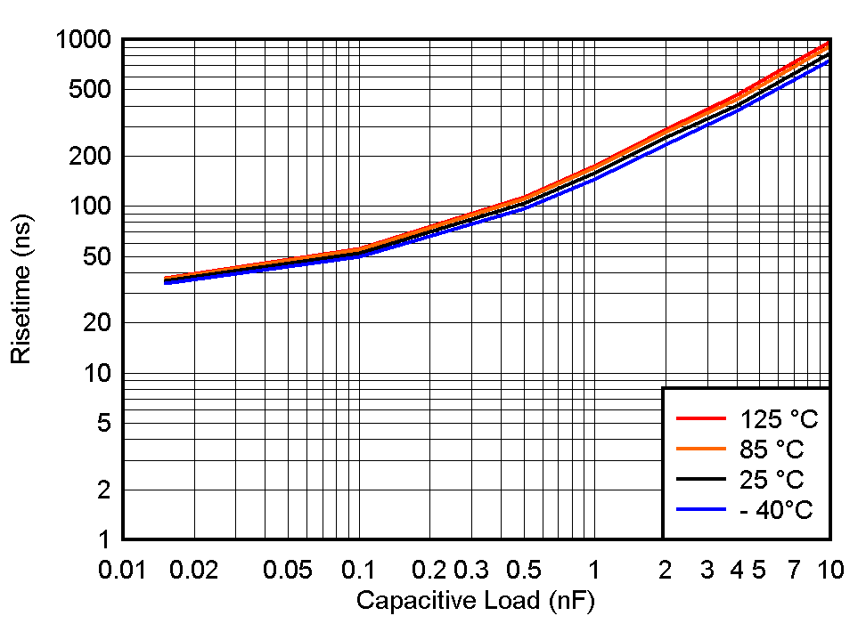
TLV1805 TR_vs_CL_3p3V.gif
VS = 3.3 V
Figure 51. tRISE vs. Capacitive Load
at 3.3V
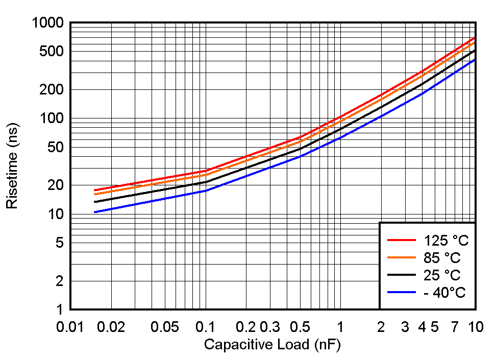
TLV1805 TR_vs_CL_5V.gif
VS = 5 V
Figure 53. tRISE vs. Capacitive Load
at 5V
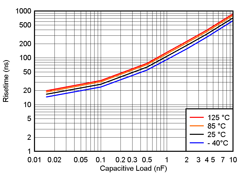
TLV1805 TR_vs_CL_12V.gif
VS = 12 V
Figure 55. tRISE vs. Capacitive Load
at 12V
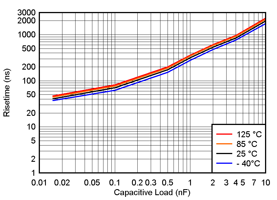
TLV1805 TR_vs_CL_40V.gif
VS = 40 V
Figure 57. tRISE vs. Capacitive Load
at 40V
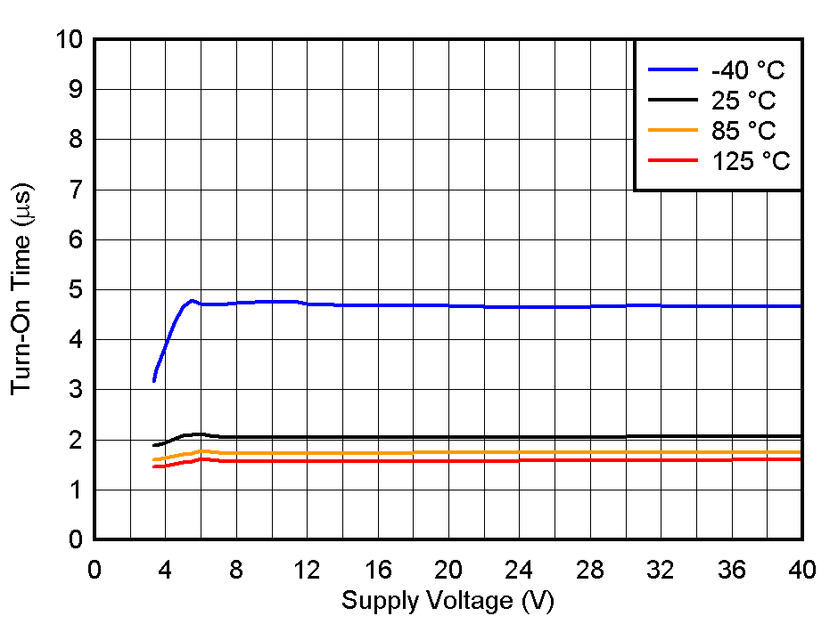
TLV1805 TON_vs_VS.gif
Figure 59. Turn-On Time vs Supply Voltage
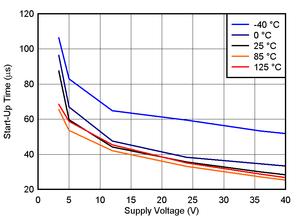
TLV1805 TSTART_vs_VS.gif
Figure 61. Start-Up Time vs Supply Voltage
TLV1805 VIO_HIST.gif
Figure 4. Offset Voltage Histogram
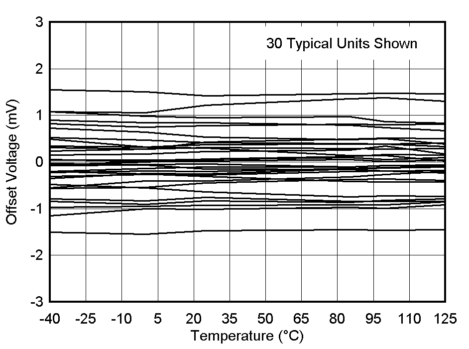
TLV1805 VIO_vs_TA.gif
Figure 6. Offset Voltage vs Temperature
TLV1805 IQ_vs_VS_OUTHI.gif
VCM = V- Output High (VID = 0.1 V)
Figure 8. Supply Current vs. Temperature, Output High
TLV1805 IB_vs_VCM_125C.gif
TA = 125 °C
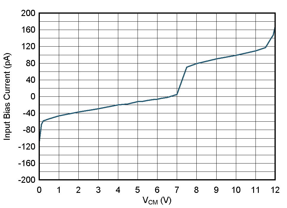
Figure 10. Input Bias Current vs. Common Mode, 125°C
TLV1805 IB_vs_VCM_n40C.gif
TA = -40 °C
Figure 12. Input Bias Current vs. Common Mode, -40°C
TLV1805 IQsd_vs_VS.gif
VCM = V-
Figure 14. Shutdown Supply Current vs. Supply Votlage
TLV1805 SDVLO_vs_TA.gif
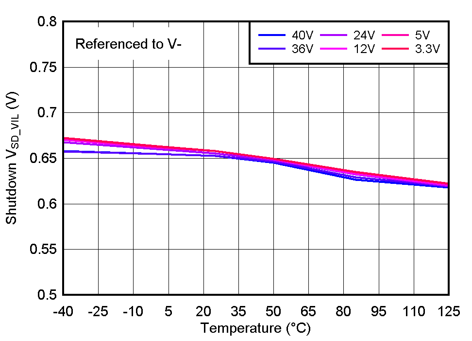
Figure 16. Shutdown Voltage Low Threshold vs. Temperature
TLV1805 SDVLO_vs_VS.gif
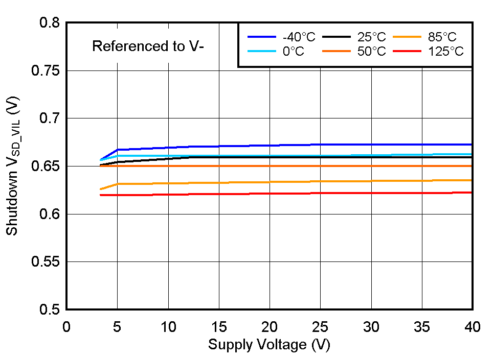
Figure 18. Shutdown Voltage Low Threshold vs. Supply Voltage
TLV1805 SDIB_vs_VSD_12V_25_n40.gif
Figure 20. Shutdown Input Bias Current vs. Shutdown Input Voltage, Low Temperatures
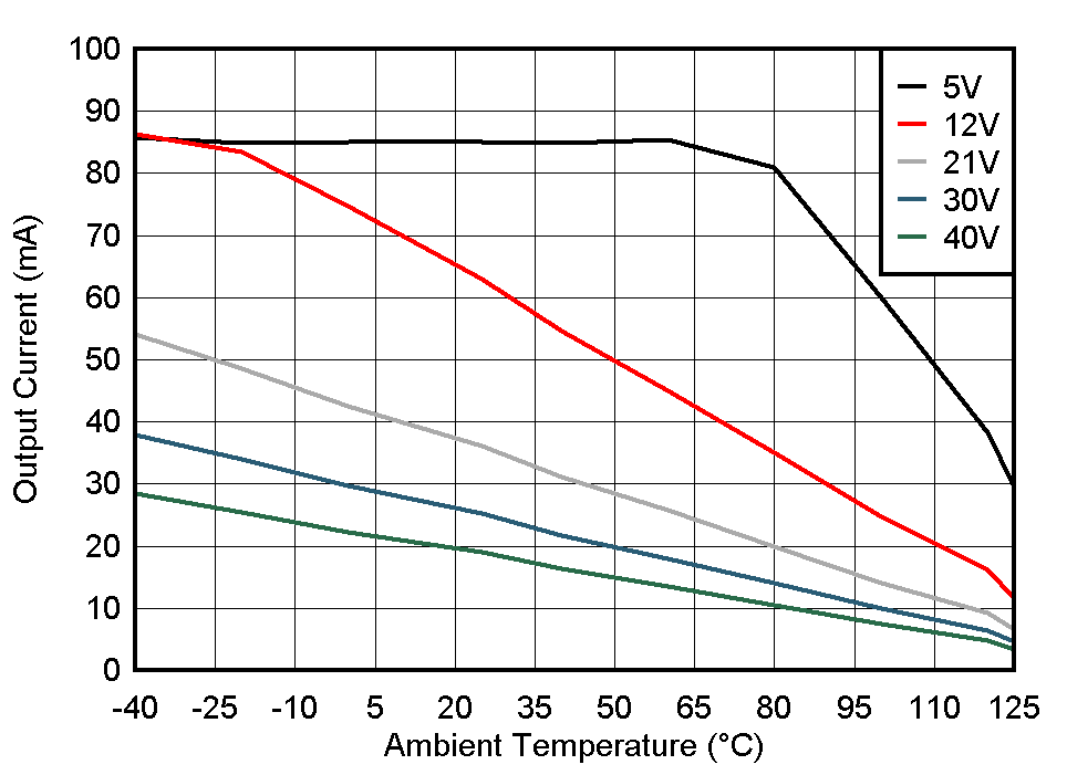
TLV1805 Detrating.gif
DBV SOT-23-6 Package
Figure 22. Maximum Output Current vs. Ambient Temperature
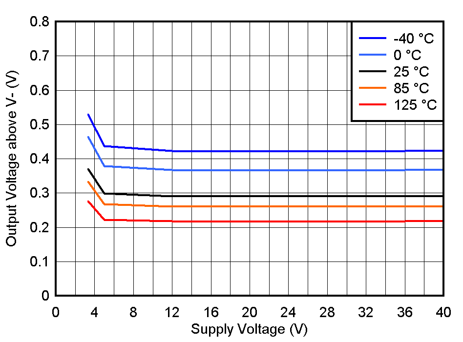
TLV1805 VOL_vs_Vs.gif
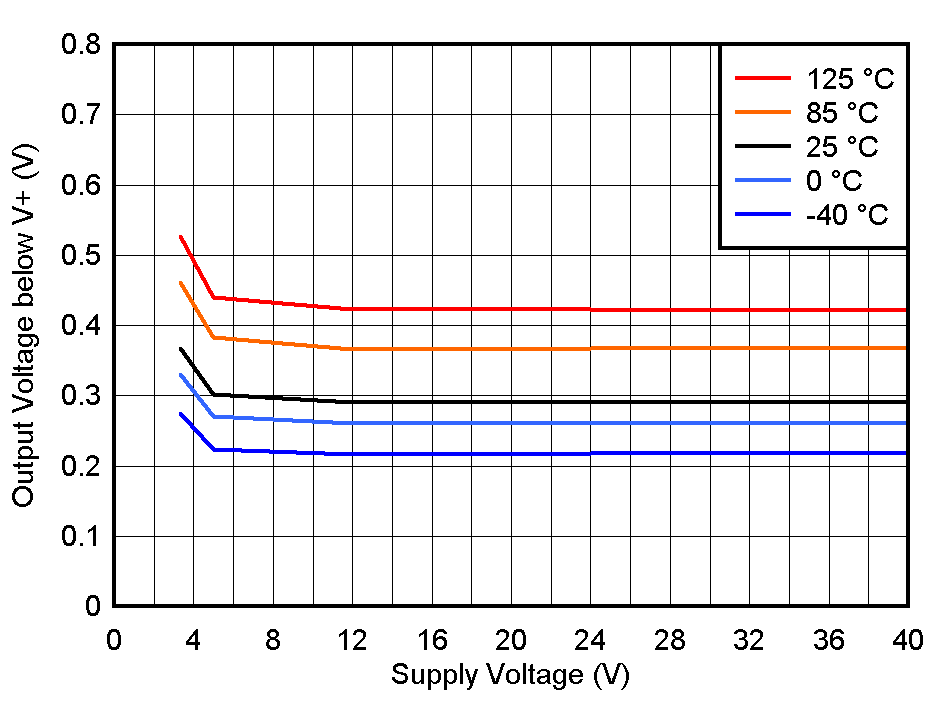
ISINK = 1 mA
Figure 24. Output Low Voltage vs. Supply Voltage
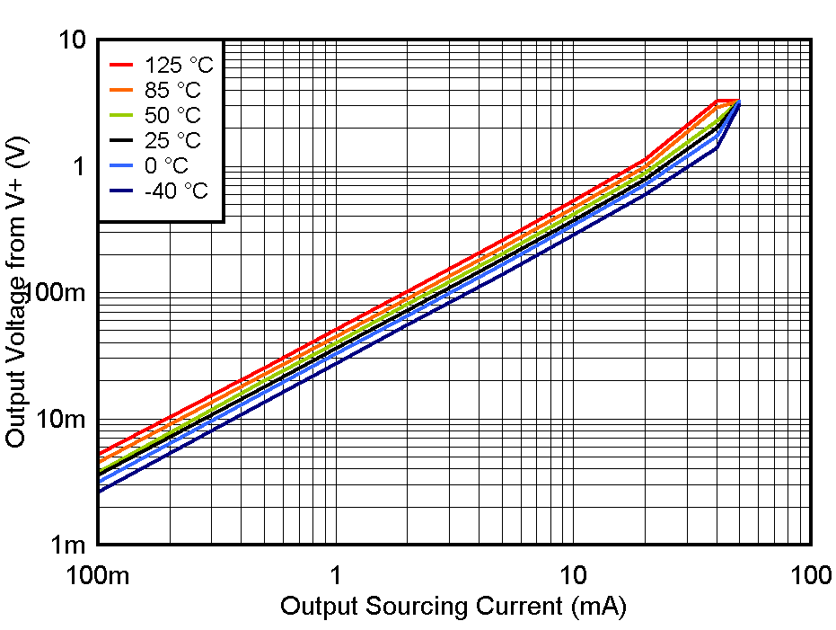
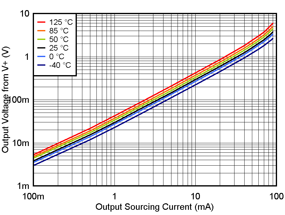
TLV1805 VOH_vs_IO_Vs3p3.gif
VS = 3.3 V
Figure 26. Output Sourcing Current vs. Output Voltage
at 3.3V
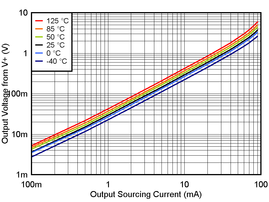
TLV1805 VOH_vs_IO_Vs12.gif
VS = 12 V
Figure 28. Output Sourcing Current vs. Output Voltage
at 12V
TLV1805 VOH_vs_IO_Vs40.gif
VS = 40 V
Figure 30. Output Sourcing Current vs. Output Voltage
at 40V
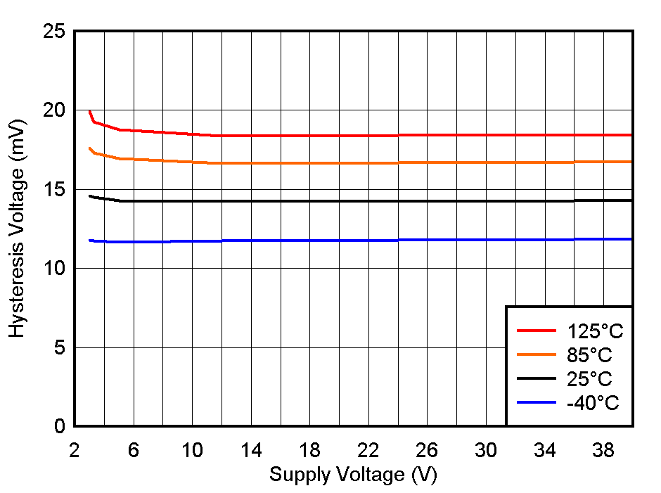
TLV1805 HYST_vs_VS.gif
Figure 32. Hysteresis vs. Supply Voltage
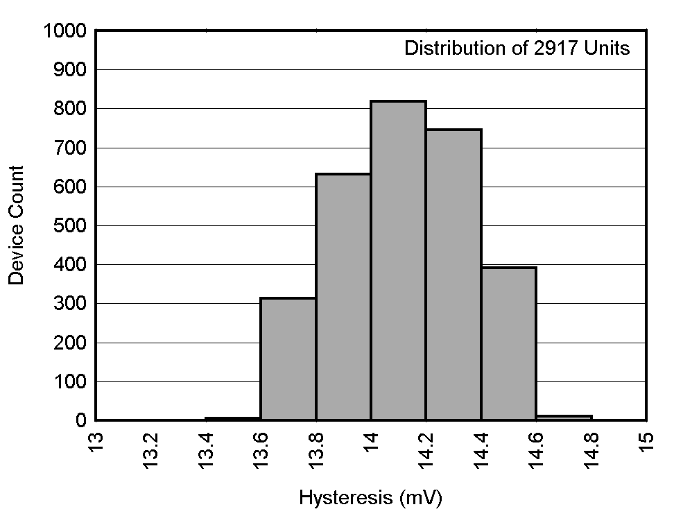
TLV1805 HYST_HIST.gif
Figure 34. Hysteresis Histogram
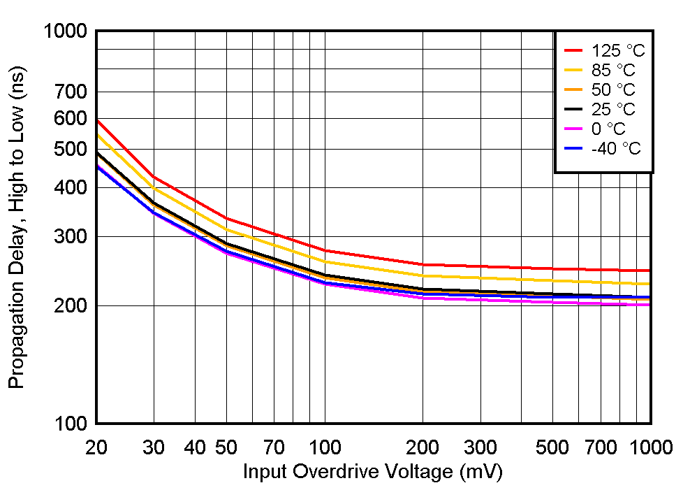
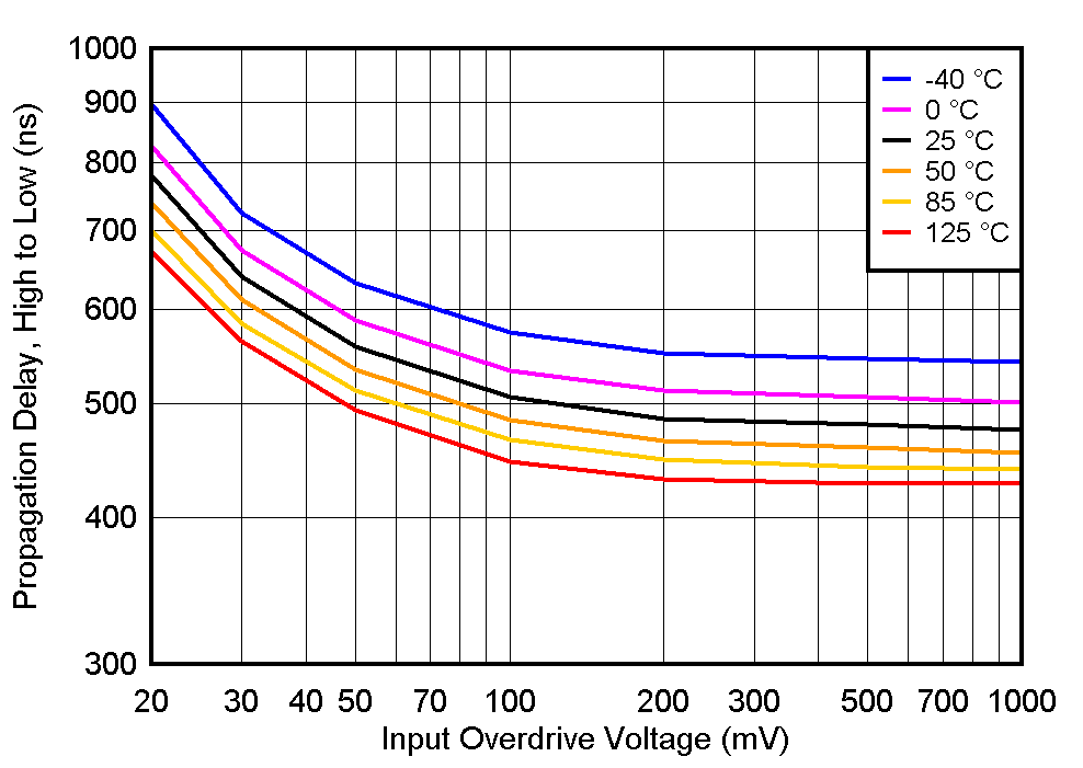
TLV1805 TPHL_vs_VOD_Vs3p3.gif
VS = 3.3 V CL = 15pF
Figure 36. TPHL Response Time vs. Overdrive
at 3.3V
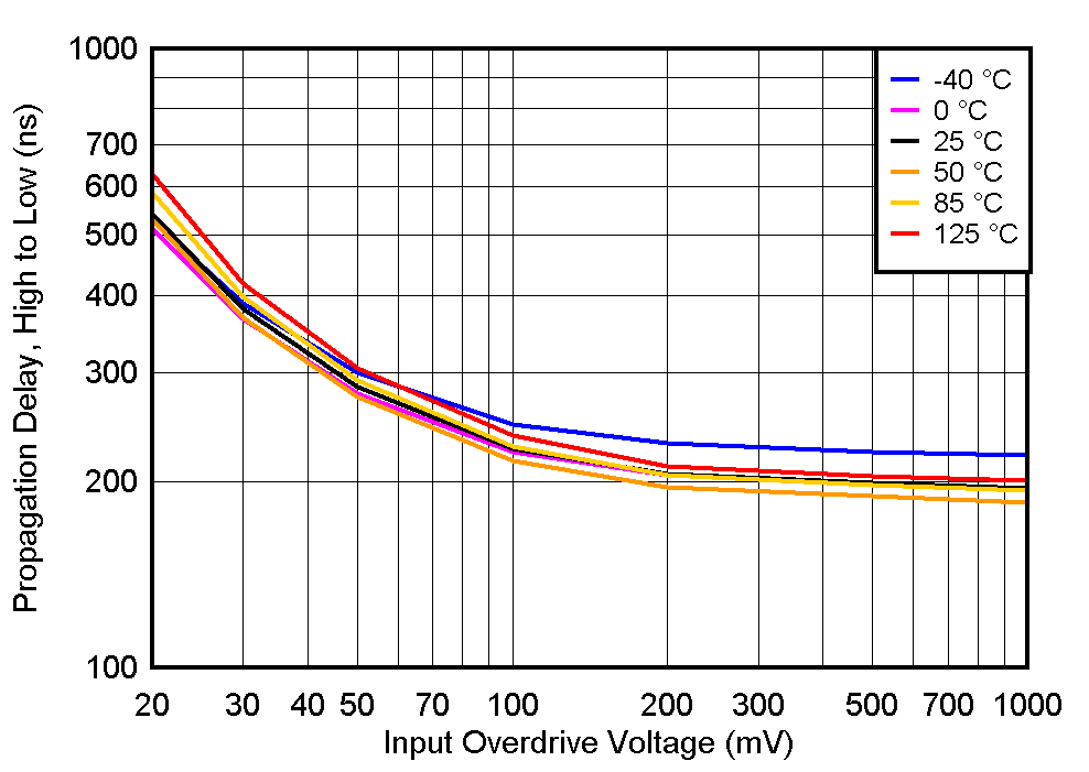
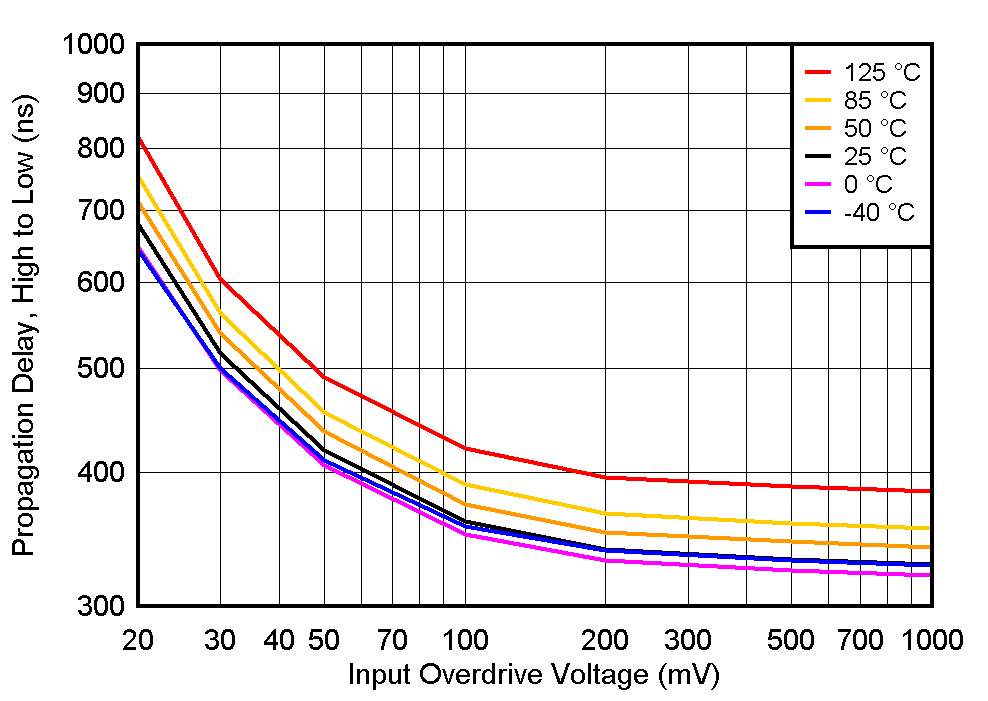
TLV1805 TPHL_vs_VOD_Vs5.gif
VS = 5 V CL = 15pF
Figure 38. TPHL Response Time vs. Overdrive
at 5V
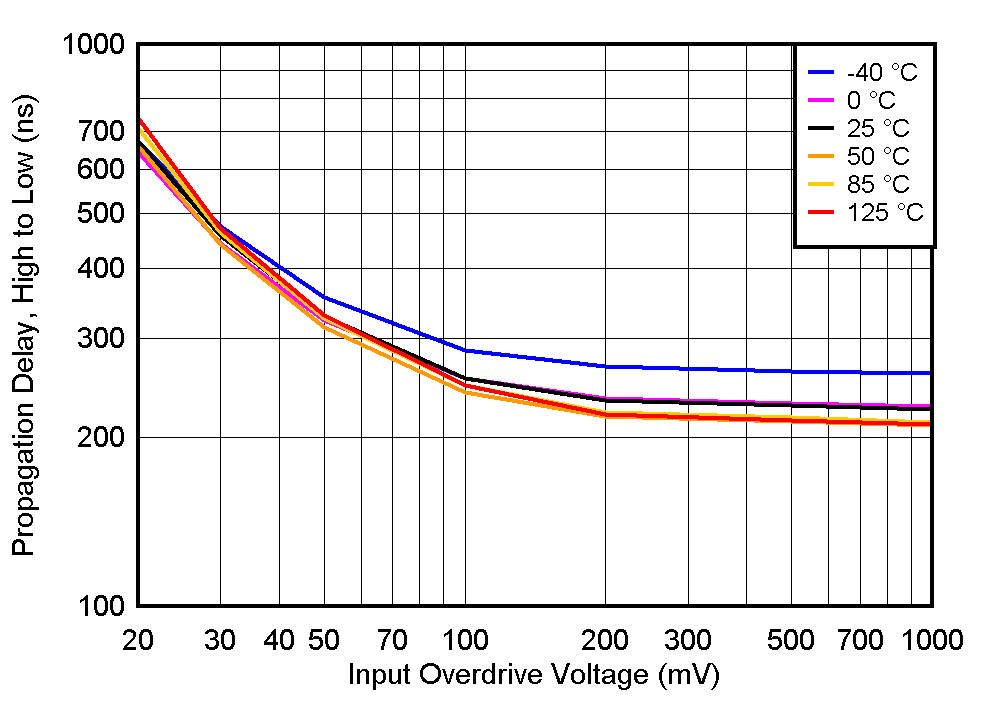
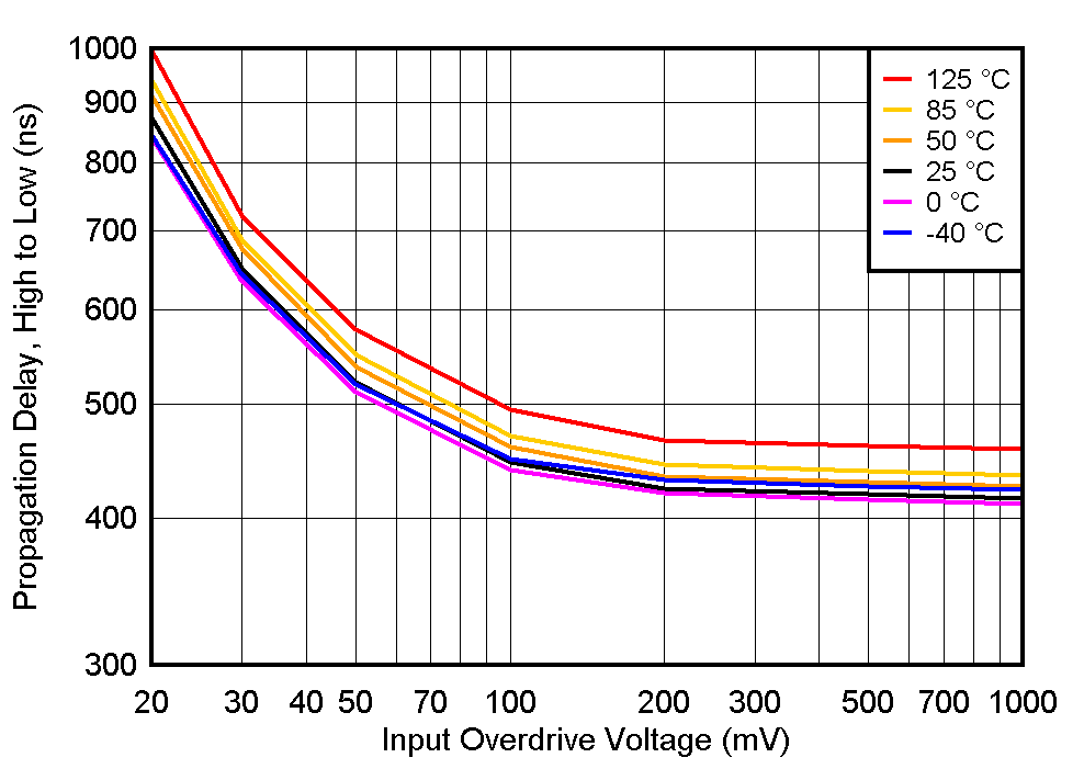
TLV1805 TPHL_vs_VOD_Vs12.gif
VS = 12 V CL = 15pF
Figure 40. TPHL Response Time vs. Overdrive
at 12V
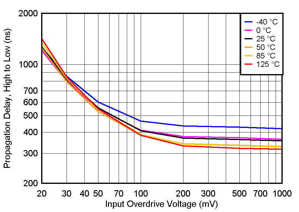
TLV1805 TPHL_vs_VOD_Vs40.gif
VS = 40 V CL = 15pF
Figure 42. TPHL Response Time vs. Overdrive
at 40V
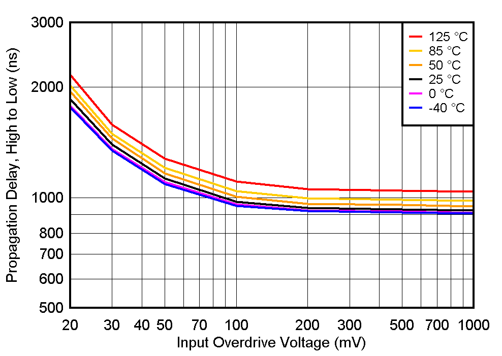
TLV1805 TPHL_vs_VOD_Vs3p3_4n.gif
VS = 3.3 V CL = 4nF
Figure 44. TPHL Response Time vs. Overdrive
at 3.3V
TLV1805 TPHL_vs_VOD_Vs5_4n.gif
VS = 5 V CL = 4nF
Figure 46. TPHL Response Time vs. Overdrive
at 5V
TLV1805 TPHL_vs_VOD_Vs12_4n.gif
VS = 12 V CL = 4nF
Figure 48. TPHL Response Time vs. Overdrive
at 12V
TLV1805 TPHL_vs_VOD_Vs40_4n.gif
VS = 40 V CL = 4nF
Figure 50. TPHL Response Time vs. Overdrive
at 40V
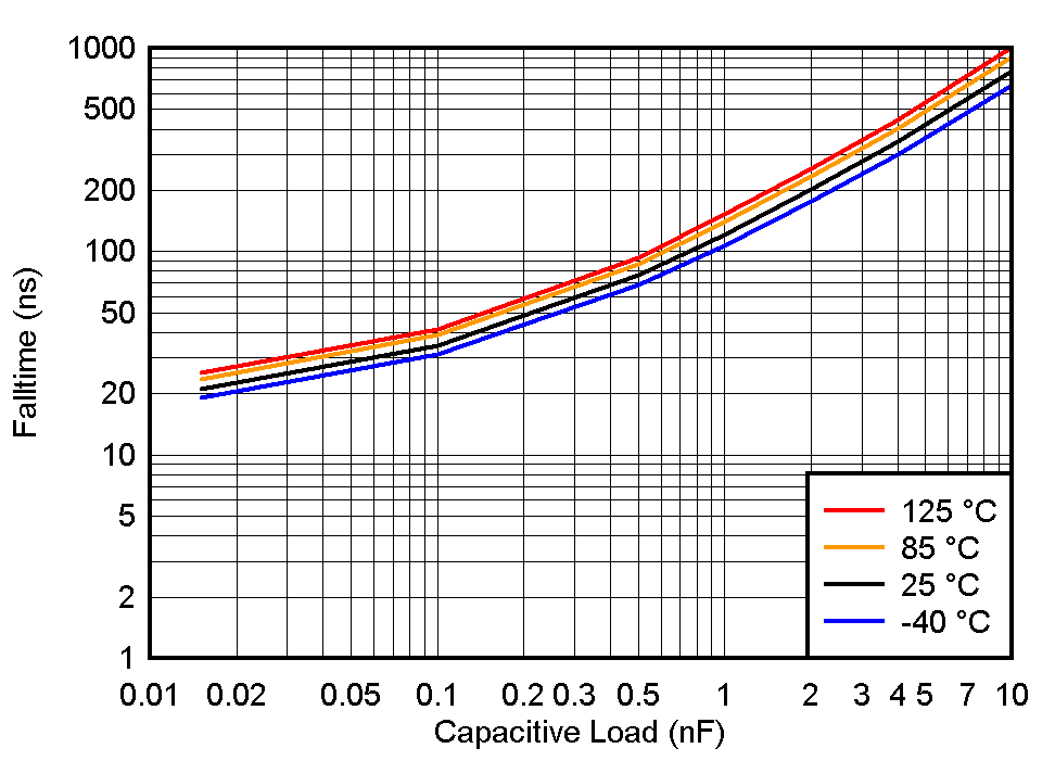
TLV1805 TF_vs_CL_3p3V.gif
VS = 3.3 V
Figure 52. tFALL vs. Capacitive Load
at 3.3V
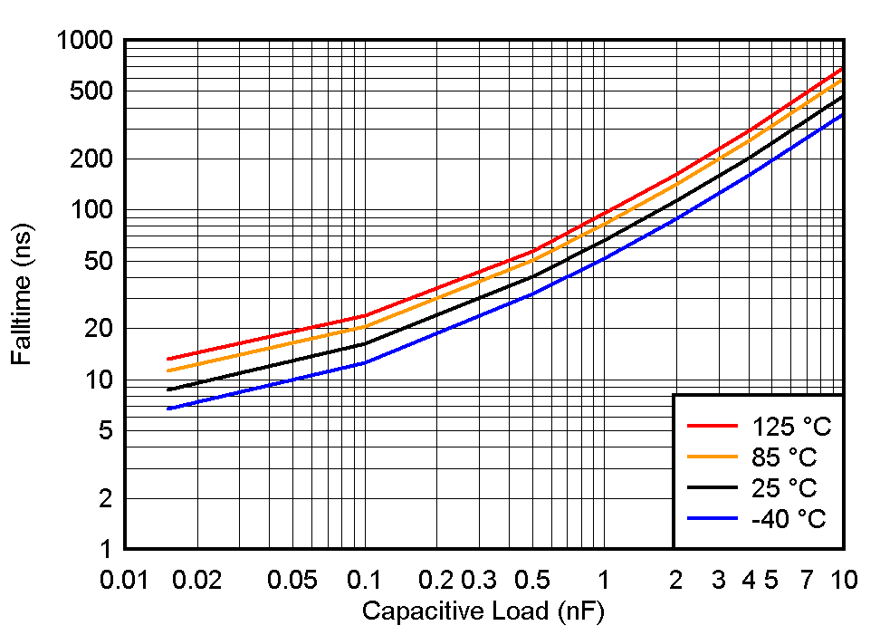
TLV1805 TF_vs_CL_5V.gif
VS = 5 V
Figure 54. tFALL vs. Capacitive Load
at 5V
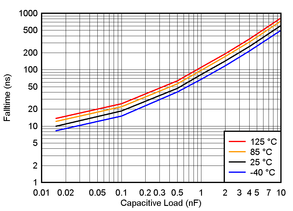
TLV1805 TF_vs_CL_12V.gif
VS = 12 V
Figure 56. tFALL vs. Capacitive Load
at 12V
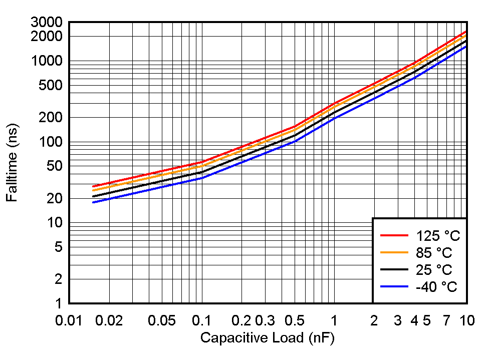
TLV1805 TF_vs_CL_40V.gif
VS = 40 V
Figure 58. tFALL vs. Capacitive Load
at 40V
TLV1805 TOFF_vs_VS.gif
Figure 60. Turn-Off Time vs Supply Voltage
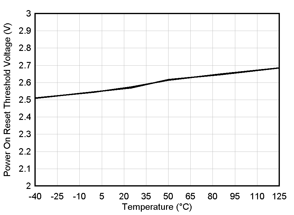
TLV1805 POR_vs_TA.gif
Figure 62. Power On Reset Voltage vs. Temperature