ZHCSJ63 December   2018 TLV1805

PRODUCTION DATA.  

  1. 特性
  2. 应用
  3. 说明
    1.     Device Images
      1.      采用 P 沟道 MOSFET 的过压保护
      2.      采用 P 沟道 MOSFET 的反向电流和过压保护
  4. 修订历史记录
  5. 说明 (续)
  6. Pin Configuration and Functions
    1.     Pin Functions
  7. Specifications
    1. 7.1 Absolute Maximum Ratings
    2. 7.2 ESD Ratings
    3. 7.3 Recommended Operating Conditions
    4. 7.4 Thermal Information
    5. 7.5 Electrical Characteristics
    6. 7.6 Switching Characteristics
    7. 7.7 Typical Characteristics
  8. Detailed Description
    1. 8.1 Overview
    2. 8.2 Functional Block Diagram
    3. 8.3 Feature Description
      1. 8.3.1 Rail to Rail Inputs
      2. 8.3.2 Power On Reset
      3. 8.3.3 High Power Push-Pull Output
      4. 8.3.4 Shutdown Function
      5. 8.3.5 Internal Hysteresis
    4. 8.4 Device Functional Modes
      1. 8.4.1 External Hysteresis
        1. 8.4.1.1 Inverting Comparator With Hysteresis
        2. 8.4.1.2 Noninverting Comparator With Hysteresis
  9. Application and Implementation
    1. 9.1 Application Information
    2. 9.2 Typical Applications
      1. 9.2.1 Design Requirements
      2. 9.2.2 Detailed Design Procedure
      3. 9.2.3 Application Curve
      4. 9.2.4 Reverse Current Protection Using MOSFET and TLV1805
        1. 9.2.4.1 Minimum Reverse Current
        2. 9.2.4.2 N-Channel Reverse Current Protection Circuit
          1. 9.2.4.2.1 N-Channel Oscillator Circuit
      5. 9.2.5 P-Channel Reverse Current Protection Circuit
      6. 9.2.6 P-Channel Reverse Current Protection With Overvotlage Protection
      7. 9.2.7 ORing MOSFET Controller
  10. 10Power Supply Recommendations
  11. 11Layout
    1. 11.1 Layout Guidelines
    2. 11.2 Layout Example
  12. 12器件和文档支持
    1. 12.1 文档支持
      1. 12.1.1 相关文档
    2. 12.2 接收文档更新通知
    3. 12.3 社区资源
    4. 12.4 商标
    5. 12.5 静电放电警告
    6. 12.6 术语表
  13. 13机械、封装和可订购信息

封装选项

机械数据 (封装 | 引脚)
散热焊盘机械数据 (封装 | 引脚)
订购信息

Switching Characteristics

Typical values are at TA = 25°C, VS = 12 V, VCM = VS / 2; Input overdrive = 100 mV (unless otherwise noted).
PARAMETER TEST CONDITIONS MIN TYP MAX UNIT
tPHL Propagation delay time, high-to-low (1) CL = 15 pF 250 ns
CL = 4 nF 450 ns
tPLH Propagation delay time, low-to-high (1) CL = 15 pF 250 ns
CL = 4 nF 500 ns
tR Rise time 20% to 80%, CL = 15 pF 18 ns
20% to 80%, CL = 4 nF 0.3 µs
tF Fall time 20% to 80%, CL = 15 pF 10 ns
20% to 80%, CL = 4 nF 0.26 µs
tSTART Power-up time (2) 45 µs
High-to-low and low-to-high refers to the transition at the input.
During power on, VS must exceed 3.3 V for tON before the output is in a correct state.
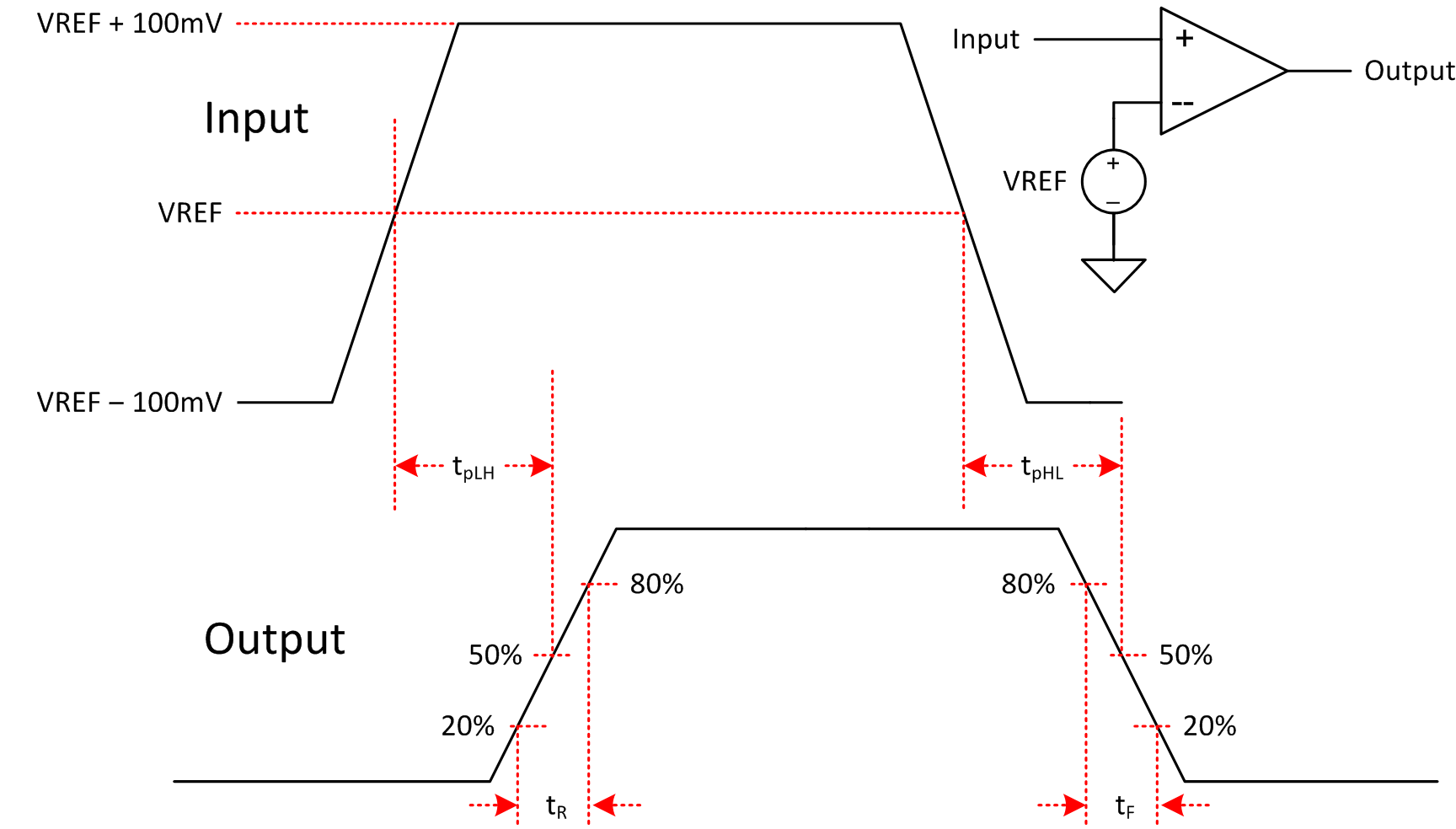
TLV1805 propdelay.tifFigure 1. Propagation Delay
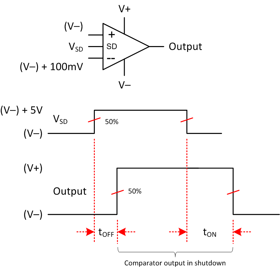
TLV1805 shutdown.tifFigure 2. Shutdown Timing