ZHCSJ09A November   2018  – November 2022 TLV1704-SEP

PRODUCTION DATA  

  1. 特性
  2. 应用
  3. 说明
  4. Revision History
  5. Pin Configuration and Functions
  6. Specifications
    1. 6.1 Absolute Maximum Ratings
    2. 6.2 ESD Ratings
    3. 6.3 Recommended Operating Conditions
    4. 6.4 Thermal Information
    5. 6.5 Electrical Characteristics
    6. 6.6 Switching Characteristics
    7. 6.7 Typical Characteristics
  7. Detailed Description
    1. 7.1 Overview
    2. 7.2 Functional Block Diagram
    3. 7.3 Feature Description
      1. 7.3.1 Comparator Inputs
      2.      19
    4. 7.4 Device Functional Modes
      1. 7.4.1 Setting Reference Voltage
  8. Application and Implementation
    1. 8.1 Application Information
    2. 8.2 Typical Application
      1. 8.2.1 Design Requirements
      2. 8.2.2 Detailed Design Procedure
      3. 8.2.3 Application Curve
    3. 8.3 Power Supply Recommendations
    4. 8.4 Layout
      1. 8.4.1 Layout Guidelines
      2. 8.4.2 Layout Example
  9. Device and Documentation Support
    1. 9.1 Documentation Support
      1. 9.1.1 Related Documentation
    2. 9.2 接收文档更新通知
    3. 9.3 支持资源
    4. 9.4 Trademarks
    5. 9.5 Electrostatic Discharge Caution
    6. 9.6 术语表
  10. 10Mechanical, Packaging, and Orderable Information

封装选项

机械数据 (封装 | 引脚)
散热焊盘机械数据 (封装 | 引脚)
订购信息

Typical Characteristics

at TA = 25°C, VS = 5 V, RPULLUP = 5.1 kΩ, and input overdrive = 100 mV (unless otherwise noted)
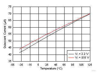
GUID-9893A038-F3DE-4C97-8A82-6FADEBDA45E8-low.gif
Figure 6-1 Quiescent Current vs Temperature
GUID-0A307C68-619E-461F-9096-4309BE2A63D5-low.gif
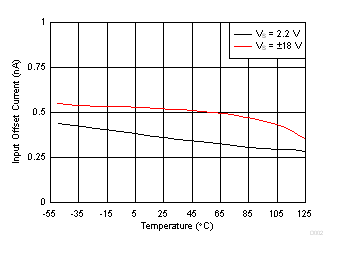
Figure 6-3 Input Offset Current vs Temperature
GUID-9FFC7CA1-97E7-4531-ACBA-386F566394B3-low.gif
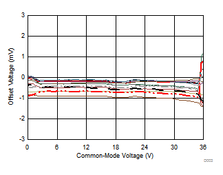
VS = ±18 V14 typical units shown
Figure 6-5 Offset Voltage vs Common-Mode Voltage
GUID-90B6F114-9782-4241-B465-D4482E3DFB93-low.gif
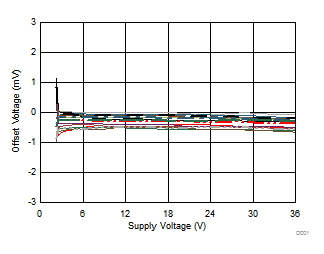
16 typical units shown
Figure 6-7 Offset Voltage vs Supply Voltage
GUID-288C0A9C-3ECB-49FA-981C-2B8F482FA56C-low.png
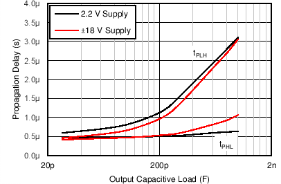
Figure 6-9 Propagation Delay vs Capacitive Load
GUID-854BE7B9-28D5-4B13-968F-90A4DA2A65E7-low.png
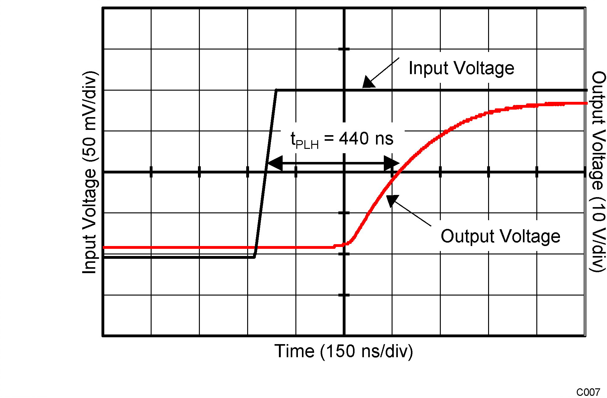
VS = 36 VOverdrive = 100 mV
Figure 6-11 Propagation Delay (TpLH)
GUID-4582F143-DC16-4BED-885A-8829FC23E8CE-low.png
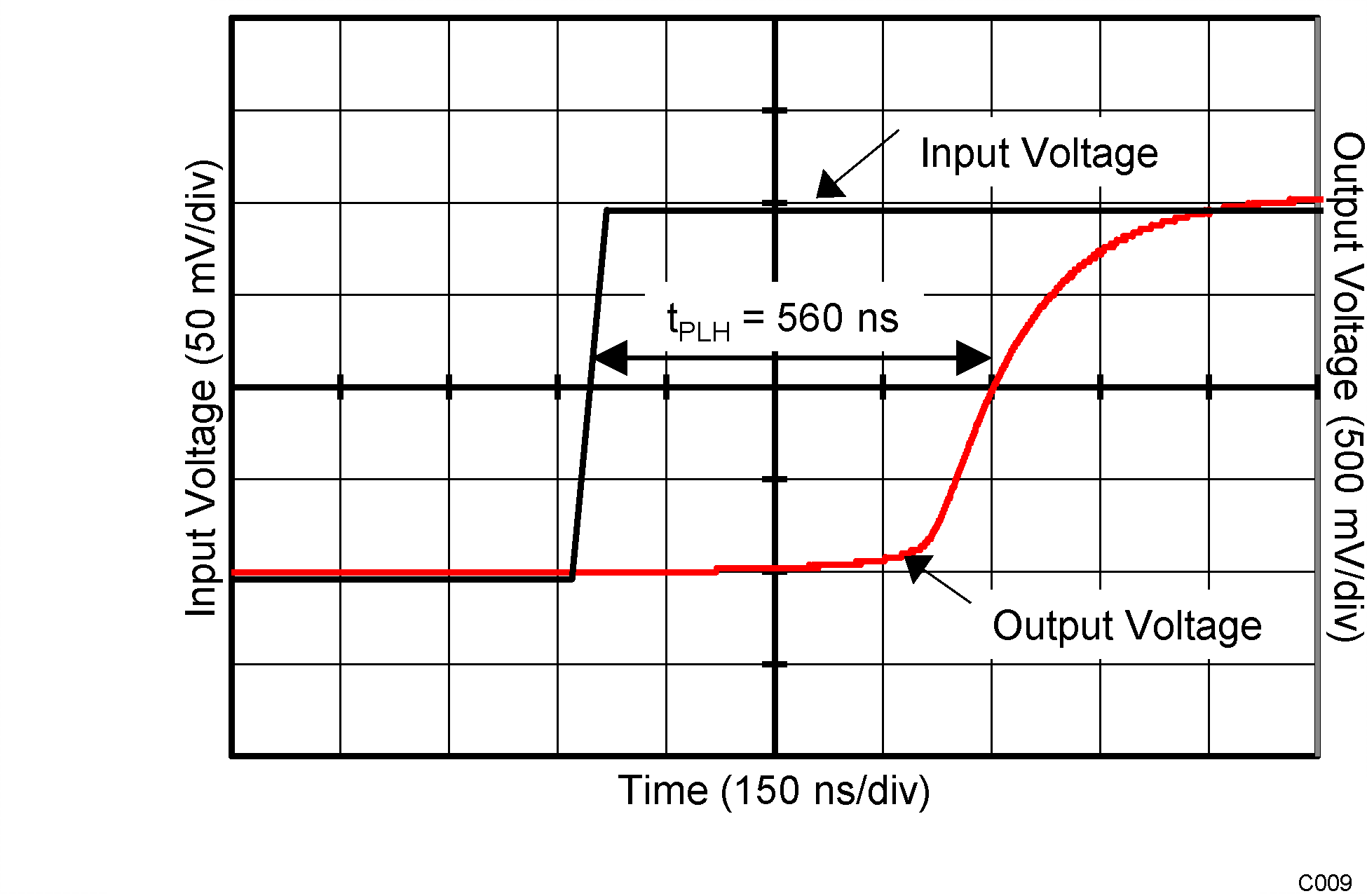
VS = 2.2 VOverdrive = 100 mV
Figure 6-13 Propagation Delay (TpLH)
GUID-2495771B-4D40-4A1B-9A65-2712DE255382-low.gif
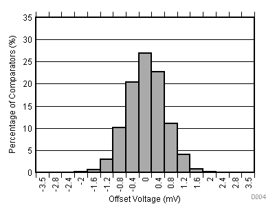
VS = ±18 VDistribution taken from 2524 comparators
Figure 6-15 Offset Voltage Production Distribution
GUID-B920BC89-A3E3-4FD4-B772-C19D05698876-low.png
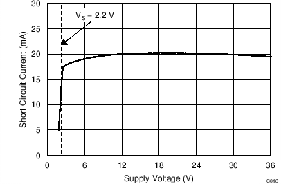
Sink current
Figure 6-17 Short-Circuit Current vs Supply Voltage
GUID-DA564587-BCD5-42CB-8076-19E7FDF25849-low.gif
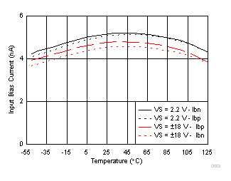
Figure 6-2 Input Bias Current vs Temperature
GUID-663E79DF-3CF7-4A88-A741-3CEEF76ACC96-low.png
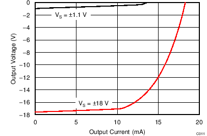
Figure 6-4 Output Voltage vs Output Current
GUID-26056D96-66F8-4BFE-AECA-D1FAB09DA7F7-low.gif
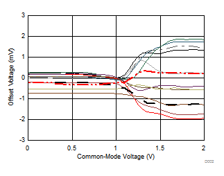
VS = 2.2 V13 typical units shown
Figure 6-6 Offset Voltage vs Common-Mode Voltage
GUID-0699BE60-15A2-4450-A12D-ABD867B5A655-low.png
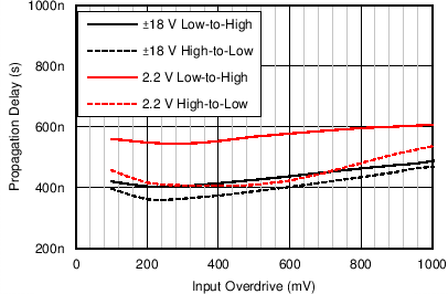
Figure 6-8 Propagation Delay vs Input Overdrive
GUID-C4D4451B-B57E-4C55-899C-6AF14897CA93-low.gif
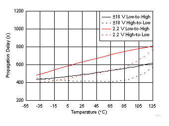
VOD = 100 mV
Figure 6-10 Propagation Delay vs Temperature
GUID-A1139408-6BE1-4175-9099-A01AFB03C82B-low.png
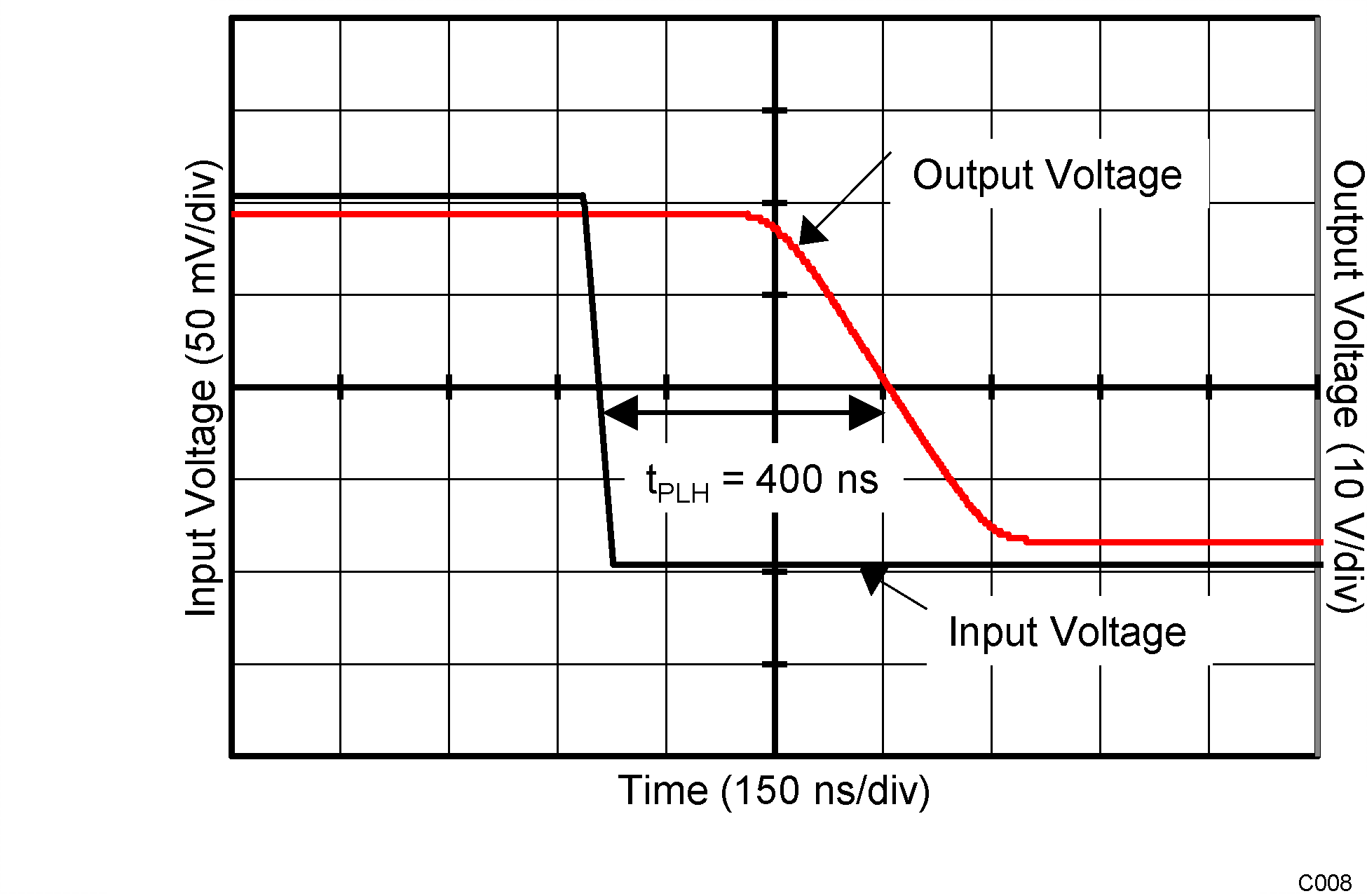
VS = 36 VOverdrive = 100 mV
Figure 6-12 Propagation Delay (TpHL)
GUID-B48BB899-D32A-4AF6-A3E3-6FBC425710E1-low.png
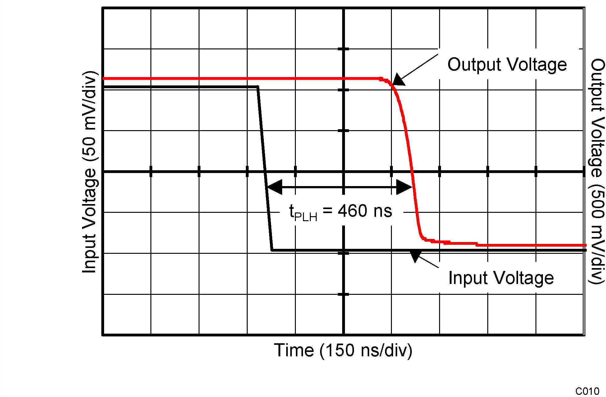
VS = 2.2 VOverdrive = 100 mV
Figure 6-14 Propagation Delay (TpHL)
GUID-2915FCBF-7D9A-4E84-A810-7F28F4E55264-low.gif
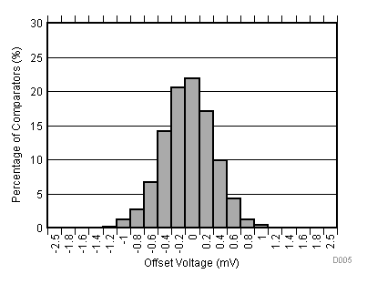
VS = 2.2 VDistribution taken from 2524 comparators
Figure 6-16 Offset Voltage Production Distribution