ZHCSE91C September 2015 – June 2017 TL16C752D
PRODUCTION DATA.
- 1 特性
- 2 应用
- 3 说明
- 4 修订历史记录
- 5 说明 (续)
- 6 Pin Configurations and Function
- 7 Specifications
-
8 Detailed Description
- 8.1 Overview
- 8.2 Functional Block Diagrams
- 8.3
Feature Description
- 8.3.1
Functional Description
- 8.3.1.1 Trigger Levels
- 8.3.1.2 Hardware Flow Control
- 8.3.1.3 Auto-RTS
- 8.3.1.4 Auto-CTS
- 8.3.1.5 Software Flow Control
- 8.3.1.6 Software Flow Control Example
- 8.3.1.7 Reset
- 8.3.1.8 Interrupts
- 8.3.1.9 Interrupt Mode Operation
- 8.3.1.10 Polled Mode Operation
- 8.3.1.11 Break and Timeout Conditions
- 8.3.1.12 Programmable Baud Rate Generator
- 8.3.1
Functional Description
- 8.4 Device Functional Modes
- 8.5
Register Maps
- 8.5.1 Principals of Operation
- 8.5.2 Receiver Holding Register (RHR)
- 8.5.3 Transmit Holding Register (THR)
- 8.5.4 FIFO Control Register (FCR)
- 8.5.5 Line Control Register (LCR)
- 8.5.6 Line Status Register (LSR)
- 8.5.7 Modem Control Register (MCR)
- 8.5.8 Modem Status Register (MSR)
- 8.5.9 Interrupt Enable Register (IER)
- 8.5.10 Interrupt Identification Register (IIR)
- 8.5.11 Enhanced Feature Register (EFR)
- 8.5.12 Divisor Latches (DLL, DLH)
- 8.5.13 Transmission Control Register (TCR)
- 8.5.14 Trigger Level Register (TLR)
- 8.5.15 FIFO Ready Register
- 8.5.16 Alternate Function Register (AFR)
- 8.5.17 RS-485 Mode
- 8.5.18 IrDA Overview
- 8.5.19 IrDA Encoder Function
- 9 Application and Implementation
- 10Power Supply Recommendations
- 11Layout
- 12器件和文档支持
- 13机械、封装和可订购信息
11 Layout
11.1 Layout Guidelines
Traces, Vias, and Other PCB Components: A right angle in a trace can cause more radiation. The capacitance increases in the region of the corner, and the characteristic impedance changes. This impedance change causes reflections.
- Avoid right-angle bends in a trace and try to route them at least with two 45° corners. To minimize any impedance change, the best routing would be a round bend (see Figure 24).
- Separate high-speed signals (for example, clock signals) from low-speed signals and digital from analog signals; again, placement is important.
- To minimize crosstalk not only between two signals on one layer but also between adjacent layers, route them with 90° to each other
Figure 44. Layout Do's and Don'ts
11.2 Layout Examples
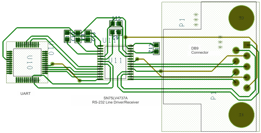
 Figure 45. RS232 Channel Layout Example
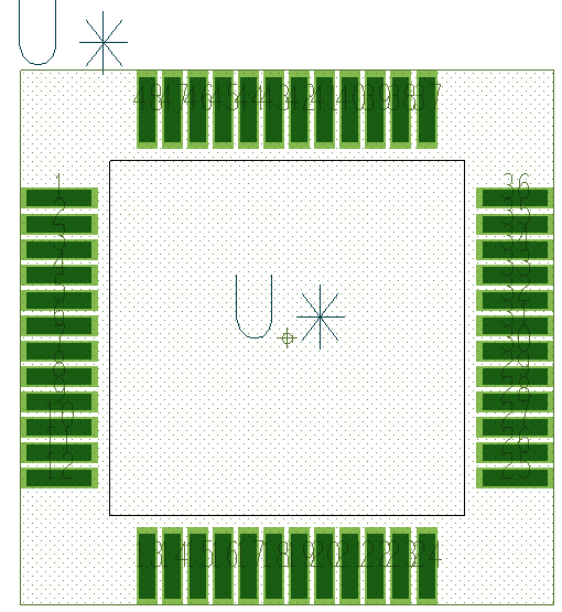
 Figure 46. Footprint Example